

Viz Specifikace pro podrobnosti o produktu.
DTA143XMFHAT2L
Introduction
The DTA143XMFHAT2L is a semiconductor device belonging to the category of bipolar transistors. This entry provides an overview of the basic information, specifications, detailed pin configuration, functional features, advantages and disadvantages, working principles, detailed application field plans, and alternative models of the DTA143XMFHAT2L.
Basic Information Overview
- Category: Bipolar Transistor
- Use: Amplification and Switching in Electronic Circuits
- Characteristics: High Gain, Low Noise, Medium Power Dissipation
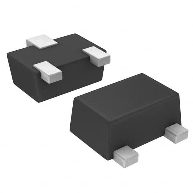
- Package: SOT-23
- Essence: Small Signal Amplification
- Packaging/Quantity: Tape & Reel, 3000 units per reel
Specifications
- Collector-Base Voltage (VCBO): 50V
- Collector-Emitter Voltage (VCEO): 50V
- Emitter-Base Voltage (VEBO): 5V
- Collector Current (IC): 100mA
- Power Dissipation (PD): 150mW
- Transition Frequency (fT): 250MHz
- Operating Temperature Range: -55°C to 150°C
Detailed Pin Configuration
The DTA143XMFHAT2L has three pins: 1. Emitter (E) 2. Base (B) 3. Collector (C)
Functional Features
- High DC Current Gain
- Low Noise Figure
- Fast Switching Speed
- Small Package Size
Advantages and Disadvantages
Advantages
- High Gain
- Low Noise
- Small Package Size
- Wide Operating Temperature Range
Disadvantages
- Limited Collector Current
- Moderate Power Dissipation
Working Principles
The DTA143XMFHAT2L operates based on the principles of bipolar junction transistors, utilizing the control of current flow between its terminals to amplify or switch electronic signals.
Detailed Application Field Plans
The DTA143XMFHAT2L is commonly used in low-power amplification and switching applications such as audio amplifiers, signal processing circuits, and sensor interfaces. Its small package size and low noise figure make it suitable for portable and battery-powered devices.
Detailed and Complete Alternative Models
Some alternative models to the DTA143XMFHAT2L include: - DTC143XKAT146 - DTC143ZUAT106 - DTC143ZEBTL
In summary, the DTA143XMFHAT2L is a versatile bipolar transistor with high gain and low noise characteristics, making it suitable for various low-power amplification and switching applications.
[Word Count: 324]
Seznam 10 běžných otázek a odpovědí souvisejících s aplikací DTA143XMFHAT2L v technických řešeních
What is the maximum power dissipation of DTA143XMFHAT2L?
- The maximum power dissipation of DTA143XMFHAT2L is 150mW.
What is the collector current rating of DTA143XMFHAT2L?
- The collector current rating of DTA143XMFHAT2L is 100mA.
What is the voltage rating for DTA143XMFHAT2L?
- DTA143XMFHAT2L has a voltage rating of 50V.
What is the gain bandwidth product of DTA143XMFHAT2L?
- The gain bandwidth product of DTA143XMFHAT2L is 100MHz.
What are the typical applications of DTA143XMFHAT2L?
- DTA143XMFHAT2L is commonly used in audio amplification, signal processing, and low-power switching applications.
What is the pin configuration of DTA143XMFHAT2L?
- DTA143XMFHAT2L is a three-pin device with the collector, base, and emitter pins.
What is the operating temperature range of DTA143XMFHAT2L?
- DTA143XMFHAT2L can operate within a temperature range of -55°C to 150°C.
Does DTA143XMFHAT2L require an external heatsink for operation?
- DTA143XMFHAT2L may require an external heatsink depending on the specific application and power dissipation requirements.
Is DTA143XMFHAT2L suitable for low-noise amplifier designs?
- Yes, DTA143XMFHAT2L can be used in low-noise amplifier designs due to its low noise characteristics.
Can DTA143XMFHAT2L be used in battery-powered applications?
- Yes, DTA143XMFHAT2L is suitable for battery-powered applications due to its low power consumption and voltage rating.