

Viz Specifikace pro podrobnosti o produktu.
SI5330G-B00218-GMR
Basic Information Overview
- Category: Integrated Circuit (IC)
- Use: Clock Generator and Multiplier
- Characteristics:
- High-frequency performance
- Low jitter
- Programmable output frequencies
- Small package size
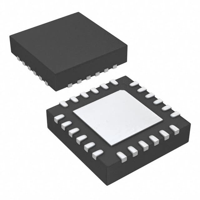
- Package: QFN (Quad Flat No-leads)
- Essence: Clock generation and multiplication
- Packaging/Quantity: Tape and Reel, 2500 units per reel
Specifications and Parameters
- Input Voltage Range: 1.8V to 3.3V
- Output Frequency Range: 1kHz to 710MHz
- Number of Outputs: 4
- Supply Current: 75mA
- Operating Temperature Range: -40°C to +85°C
Detailed Pin Configuration
The SI5330G-B00218-GMR has a total of 20 pins. The pin configuration is as follows:
| Pin Number | Pin Name | Description | |------------|----------|-------------| | 1 | VDD | Power supply voltage input | | 2 | GND | Ground | | 3 | XAXB | Differential clock input | | 4 | XAXA | Differential clock input | | 5 | XBXB | Differential clock input | | 6 | XBXC | Differential clock input | | 7 | XBYB | Differential clock input | | 8 | XBYC | Differential clock input | | 9 | XCYC | Differential clock input | | 10 | XCZC | Differential clock input | | 11 | YBYC | Differential clock input | | 12 | YCZC | Differential clock input | | 13 | ZCZD | Differential clock input | | 14 | ZDZE | Differential clock input | | 15 | VDD | Power supply voltage input | | 16 | GND | Ground | | 17 | OUT0 | Clock output 0 | | 18 | OUT1 | Clock output 1 | | 19 | OUT2 | Clock output 2 | | 20 | OUT3 | Clock output 3 |
Functional Characteristics
- Clock Generation: The SI5330G-B00218-GMR generates high-frequency clock signals based on the input differential clock signals.
- Clock Multiplication: It can multiply the input clock frequency to provide higher-frequency clock outputs.
- Programmable Output Frequencies: The device allows programming of the output frequencies through configuration registers.
- Low Jitter: The IC ensures low jitter in the generated clock signals, resulting in improved signal integrity.
Advantages and Disadvantages
Advantages: - High-frequency performance - Low jitter - Small package size - Programmable output frequencies
Disadvantages: - Limited number of outputs (4)
Applicable Range of Products
The SI5330G-B00218-GMR is suitable for applications that require high-frequency clock generation and multiplication. It finds applications in various industries, including telecommunications, networking, data centers, and consumer electronics.
Working Principles
The SI5330G-B00218-GMR utilizes a phase-locked loop (PLL) architecture to generate and multiply clock signals. The input differential clock signals are processed by the PLL circuitry, which generates the desired output frequencies based on the programmed settings.
Detailed Application Field Plans
The SI5330G-B00218-GMR can be used in the following application fields: 1. Telecommunications: Providing clock signals for communication systems and network equipment. 2. Networking: Clock generation and synchronization in routers, switches, and other network devices. 3. Data Centers: Clock distribution and synchronization in server farms and data storage systems. 4. Consumer Electronics: Clock generation for audio/video equipment, gaming consoles, and set-top boxes.
Detailed Alternative Models
Some alternative models to the SI5330G-B00218-GMR include: - SI5338G-B00218-GMR - SI5341G-B00218-GMR - SI5361G-B00218-GMR - SI5381G-B00218-GMR - SI5391G-B00218-GMR
5 Common Technical Questions and Answers
Q: What is the maximum output frequency of the SI5330G-B00218-GMR? A: The maximum output frequency is 710MHz.
Q: Can I power the IC with a voltage higher than 3.3V? A: No, the recommended input voltage range is 1.8V to 3.3V.
Q: How many clock outputs does the SI5330G-B00218-GMR have? A