

Viz Specifikace pro podrobnosti o produktu.
SI5338E-A-GM
Overview
- Category: Integrated Circuit
- Use: Clock Generator and Multiplier
- Characteristics: High-performance, low-jitter, programmable clock generator
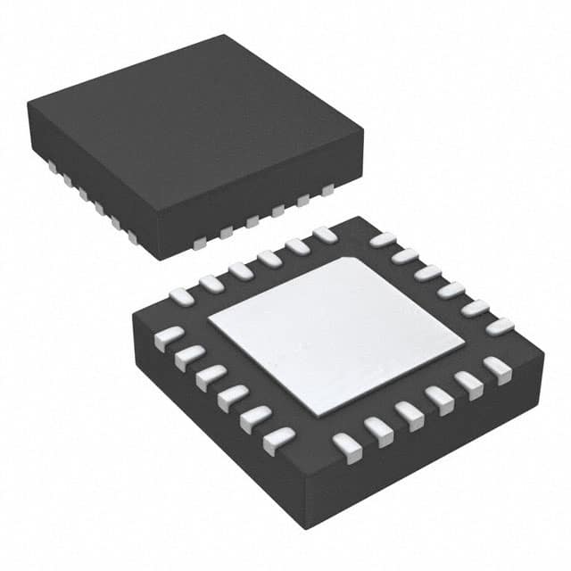
- Package: 24-pin QFN
- Essence: Provides multiple clock outputs with precise frequency control
- Packaging/Quantity: Tape and Reel, 2500 units per reel
Specifications and Parameters
- Input Voltage Range: 2.375V to 3.63V
- Output Frequency Range: 1kHz to 945MHz
- Output Format: LVPECL, LVDS, HCSL, CMOS
- Programmable Features: Output frequency, output format, spread spectrum modulation, phase jitter reduction
- Operating Temperature Range: -40°C to +85°C
Pin Configuration
The SI5338E-A-GM has a total of 24 pins. The pin configuration is as follows:
| Pin Number | Pin Name | Description | |------------|----------|-------------| | 1 | VDDO | Output Power Supply Voltage | | 2 | VDD | Core Power Supply Voltage | | 3 | GND | Ground | | 4 | XAXB | Differential Clock Input | | 5 | XAXA | Differential Clock Input | | 6 | XBXB | Differential Clock Input | | 7 | XBXA | Differential Clock Input | | 8 | CLKIN | Single-Ended Clock Input | | 9 | SDA | I2C Serial Data Input | | 10 | SCL | I2C Serial Clock Input | | 11-14 | OUT0-OUT3 | Clock Outputs | | 15-18 | OUT4-OUT7 | Clock Outputs | | 19-22 | OUT8-OUT11 | Clock Outputs | | 23-24 | NC | No Connection |
Functional Characteristics
- High-frequency clock generation and multiplication
- Programmable output frequencies with fine resolution
- Low phase noise and jitter
- Spread spectrum modulation for EMI reduction
- Phase jitter reduction for improved signal integrity
Advantages and Disadvantages
Advantages: - Wide input voltage range - Flexible output format options - Precise frequency control - Low phase noise and jitter
Disadvantages: - Requires I2C interface for configuration - Limited number of clock outputs
Applicable Range of Products
The SI5338E-A-GM is suitable for various applications that require high-performance clock generation and multiplication. It can be used in telecommunications, networking, data centers, industrial automation, and consumer electronics.
Working Principles
The SI5338E-A-GM utilizes a phase-locked loop (PLL) to generate precise clock signals. The PLL locks onto an input reference clock and generates multiple output clocks with programmable frequencies and formats. The device also incorporates spread spectrum modulation and phase jitter reduction techniques to improve signal quality.
Detailed Application Field Plans
- Telecommunications: Use the SI5338E-A-GM to generate clock signals for high-speed data transmission in communication systems.
- Networking: Employ the device to provide synchronized clock signals for network switches and routers.
- Data Centers: Utilize the SI5338E-A-GM for clock distribution in server farms and storage systems.
- Industrial Automation: Apply the device in industrial control systems that require precise timing synchronization.
- Consumer Electronics: Incorporate the SI5338E-A-GM in audio/video equipment, gaming consoles, and smart home devices for accurate timing.
Detailed Alternative Models
- SI5338A-A-GM: Similar to SI5338E-A-GM but with extended temperature range (-40°C to +105°C).
- SI5338B-A-GM: Similar to SI5338E-A-GM but with additional features for enhanced clock performance.
- SI5338C-A-GM: Similar to SI5338E-A-GM but with a different package option (32-pin QFN).
5 Common Technical Questions and Answers
Q: What is the maximum output frequency of the SI5338E-A-GM? A: The device can generate clock signals up to 945MHz.
Q: Can I program the output format of the clock signals? A: Yes, the SI5338E-A-GM supports various output formats such as LVPECL, LVDS, HCSL, and CMOS.
Q: Does the SI5338E-A-GM have any built-in EMI reduction features? A: Yes, the device offers spread spectrum modulation capability to reduce electromagnetic interference.
Q: How can I control the SI5338E-A-GM's configuration? A: