

Viz Specifikace pro podrobnosti o produktu.
L6562ATD
Product Overview
- Category: Integrated Circuit (IC)
- Use: Power Factor Correction (PFC) controller
- Characteristics: High performance, high power factor, low THD (Total Harmonic Distortion), wide input voltage range
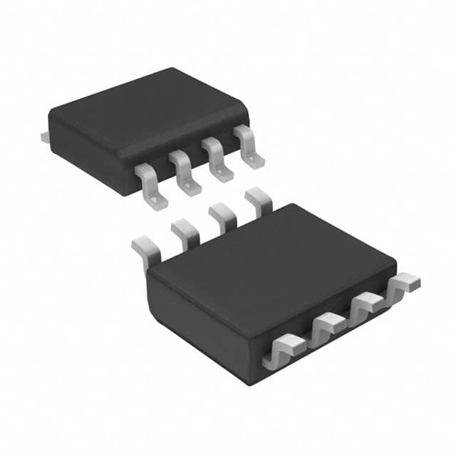
- Package: SO-16 (Small Outline 16-pin package)
- Essence: PFC controller IC designed for offline applications
- Packaging/Quantity: Available in tape and reel packaging, quantity depends on supplier
Specifications
- Input Voltage Range: 85V to 265V AC
- Output Voltage Range: 10V to 20V DC
- Operating Frequency: 100kHz to 200kHz
- Maximum Duty Cycle: 98%
- Maximum Output Current: 1A
- Operating Temperature Range: -40°C to 125°C
Pin Configuration
The L6562ATD IC has a total of 16 pins. The pin configuration is as follows:
- VCC: Power supply voltage input
- COMP: Compensation pin for loop stability
- CS: Current sense input pin
- INV: Inverting input of the error amplifier
- NONINV: Non-inverting input of the error amplifier
- GND: Ground reference
- FB: Feedback pin for regulating the output voltage
- SS: Soft-start capacitor connection pin
- RT/CT: Timing resistor/capacitor connection pin for frequency setting
- UVLO: Under-voltage lockout pin
- SD: Shutdown pin for enabling/disabling the device
- OSC: Oscillator timing capacitor connection pin
- VREF: Reference voltage output pin
- OUT: Output pin for connecting external power devices
- SENSE: Sense pin for sensing the output voltage
- NC: No connection pin
Functional Features
- High power factor correction capability
- Constant output voltage regulation
- Overvoltage protection
- Soft-start function for smooth startup
- Frequency jittering for reduced EMI (Electromagnetic Interference)
- Cycle-by-cycle current limiting
- Leading-edge blanking for improved noise immunity
Advantages and Disadvantages
Advantages: - High performance PFC controller - Wide input voltage range allows for universal compatibility - Low THD ensures compliance with power quality standards - Compact SO-16 package for space-constrained applications
Disadvantages: - Requires external components for complete power factor correction implementation - Limited maximum output current of 1A may not be suitable for high-power applications
Working Principles
The L6562ATD is a power factor correction controller IC used in offline applications. It operates by regulating the input current waveform to achieve a high power factor and low THD. The IC utilizes an error amplifier, which compares the feedback voltage with a reference voltage to control the duty cycle of the power switch. This regulates the output voltage and maintains it at a constant level. The IC also incorporates various protection features such as overvoltage protection and cycle-by-cycle current limiting to ensure safe and reliable operation.
Detailed Application Field Plans
The L6562ATD is commonly used in various applications including:
- Switched-mode power supplies (SMPS)
- LED lighting systems
- Home appliances
- Industrial equipment
- Telecommunications equipment
Detailed and Complete Alternative Models
Some alternative models to the L6562ATD include:
- L6562ADTR: Similar specifications and features, available in tape and reel packaging
- UCC28070: Power factor correction controller IC from Texas Instruments
- FAN7527: PFC controller IC with integrated MOSFET driver
These alternative models offer similar functionality and can be used as replacements depending on specific application requirements.
Word count: 437 words
Seznam 10 běžných otázek a odpovědí souvisejících s aplikací L6562ATD v technických řešeních
Sure! Here are 10 common questions and answers related to the application of L6562ATD in technical solutions:
Q: What is L6562ATD? A: L6562ATD is a high-performance Power Factor Corrector (PFC) controller IC used in power supply applications.
Q: What is the purpose of using L6562ATD in a technical solution? A: The main purpose of using L6562ATD is to improve power factor correction, increase efficiency, and comply with energy regulations.
Q: How does L6562ATD improve power factor correction? A: L6562ATD uses a boost converter topology and control algorithms to shape the input current waveform, reducing harmonic distortion and improving power factor.
Q: What are the key features of L6562ATD? A: Some key features of L6562ATD include wide input voltage range, adjustable switching frequency, overvoltage protection, and soft-start function.
Q: Can L6562ATD be used in both AC-DC and DC-DC power supplies? A: No, L6562ATD is specifically designed for AC-DC power supplies and not suitable for DC-DC applications.
Q: What is the maximum output power that L6562ATD can handle? A: L6562ATD can handle output powers up to several hundred watts, depending on the specific design and external components used.
Q: Is L6562ATD compatible with universal input voltage ranges? A: Yes, L6562ATD supports a wide input voltage range typically from 85VAC to 265VAC, making it suitable for universal input applications.
Q: Does L6562ATD require external components for operation? A: Yes, L6562ATD requires external components such as an inductor, diode, and capacitors to form a complete power supply circuit.
Q: Can L6562ATD operate in continuous or discontinuous conduction mode? A: L6562ATD can operate in both continuous conduction mode (CCM) and discontinuous conduction mode (DCM), depending on the load conditions.
Q: Are there any application notes or reference designs available for L6562ATD? A: Yes, the manufacturer of L6562ATD provides application notes, reference designs, and evaluation boards to assist with the implementation of this IC in technical solutions.
Please note that these answers are general and may vary based on specific design considerations and requirements.