

Viz Specifikace pro podrobnosti o produktu.
NAND01GW3B2AZA6E
Basic Information Overview
- Category: Integrated Circuit (IC)
- Use: Non-volatile memory storage
- Characteristics: High-density, low-power consumption
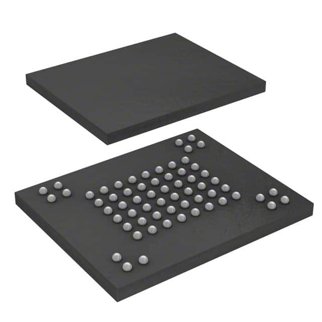
- Package: BGA (Ball Grid Array)
- Essence: NAND Flash Memory
- Packaging/Quantity: 1 piece per package
Specifications
- Capacity: 1 Gigabit (1 Gb)
- Organization: 128 Megabytes x 8 bits
- Interface: Serial Peripheral Interface (SPI)
- Supply Voltage: 2.7V - 3.6V
- Operating Temperature: -40°C to +85°C
- Data Retention: Up to 10 years
- Endurance: Up to 100,000 program/erase cycles
Detailed Pin Configuration
The NAND01GW3B2AZA6E IC has the following pin configuration:
| Pin Number | Pin Name | Description | |------------|----------|-------------| | 1 | VCC | Power supply voltage | | 2 | GND | Ground | | 3 | HOLD | Hold input for SPI operation | | 4 | WP | Write Protect input for SPI operation | | 5 | SIO0 | Serial data input/output | | 6 | SIO1 | Serial data output | | 7 | SIO2 | Serial data input/output | | 8 | SIO3 | Serial data input/output | | 9 | CS | Chip Select input for SPI operation | | 10 | CLK | Serial clock input |
Functional Features
- High-speed data transfer with SPI interface
- Efficient block management and wear-leveling algorithms
- Error correction code (ECC) for data integrity
- Support for multiple erase block sizes
- Hardware protection against accidental program/erase operations
Advantages and Disadvantages
Advantages: - High storage capacity in a compact form factor - Low power consumption, suitable for battery-powered devices - Fast data transfer rate with SPI interface - Reliable data integrity with ECC support
Disadvantages: - Limited endurance compared to other non-volatile memory technologies - Relatively higher cost per bit compared to traditional hard drives
Working Principles
The NAND01GW3B2AZA6E is based on NAND flash memory technology. It stores data by trapping electrons in a floating gate, which can be electrically programmed or erased. The IC utilizes a serial peripheral interface (SPI) for communication with the host device. It employs advanced algorithms for efficient block management, wear-leveling, and error correction to ensure reliable data storage and retrieval.
Detailed Application Field Plans
The NAND01GW3B2AZA6E IC finds applications in various electronic devices, including but not limited to: - Solid-state drives (SSDs) - USB flash drives - Memory cards (SD, microSD, etc.) - Embedded systems - Consumer electronics (smartphones, tablets, etc.)
Detailed and Complete Alternative Models
- NAND02GW3B2AZA6E: 2 Gigabit (2 Gb) capacity, same specifications as NAND01GW3B2AZA6E.
- NAND04GW3B2AZA6E: 4 Gigabit (4 Gb) capacity, same specifications as NAND01GW3B2AZA6E.
- NAND08GW3B2AZA6E: 8 Gigabit (8 Gb) capacity, same specifications as NAND01GW3B2AZA6E.
- NAND16GW3B2AZA6E: 16 Gigabit (16 Gb) capacity, same specifications as NAND01GW3B2AZA6E.
These alternative models offer higher storage capacities while maintaining compatibility with the NAND01GW3B2AZA6E in terms of pin configuration and functional features.
Word count: 346 words
Seznam 10 běžných otázek a odpovědí souvisejících s aplikací NAND01GW3B2AZA6E v technických řešeních
Sure! Here are 10 common questions and answers related to the application of NAND01GW3B2AZA6E in technical solutions:
Q: What is NAND01GW3B2AZA6E? A: NAND01GW3B2AZA6E is a specific model of NAND flash memory chip manufactured by a particular company.
Q: What is the storage capacity of NAND01GW3B2AZA6E? A: NAND01GW3B2AZA6E has a storage capacity of 1 gigabyte (GB).
Q: What is the interface used by NAND01GW3B2AZA6E? A: NAND01GW3B2AZA6E uses a standard serial peripheral interface (SPI) for communication with other devices.
Q: What is the operating voltage range of NAND01GW3B2AZA6E? A: NAND01GW3B2AZA6E operates within a voltage range of 2.7V to 3.6V.
Q: Can NAND01GW3B2AZA6E be used in industrial applications? A: Yes, NAND01GW3B2AZA6E is designed to withstand harsh environmental conditions and can be used in industrial applications.
Q: Is NAND01GW3B2AZA6E compatible with different operating systems? A: Yes, NAND01GW3B2AZA6E is compatible with various operating systems, including Windows, Linux, and embedded systems.
Q: What is the maximum data transfer rate of NAND01GW3B2AZA6E? A: NAND01GW3B2AZA6E supports a maximum data transfer rate of up to 104 megabits per second (Mbps).
Q: Can NAND01GW3B2AZA6E be used in automotive applications? A: Yes, NAND01GW3B2AZA6E is suitable for automotive applications and can withstand the temperature and vibration requirements of such environments.
Q: Does NAND01GW3B2AZA6E support hardware encryption? A: No, NAND01GW3B2AZA6E does not have built-in hardware encryption capabilities.
Q: What is the typical lifespan of NAND01GW3B2AZA6E? A: NAND flash memory chips like NAND01GW3B2AZA6E typically have a lifespan of thousands to millions of write/erase cycles, depending on usage patterns.
Please note that the answers provided here are general and may vary based on specific technical requirements and application scenarios.