

Viz Specifikace pro podrobnosti o produktu.
STH110N10F7-2: Product Overview and Analysis
Introduction
The STH110N10F7-2 is a power MOSFET belonging to the category of electronic components. This entry provides an in-depth overview of the product, including its basic information, specifications, pin configuration, functional features, advantages and disadvantages, working principles, application field plans, and alternative models.
Basic Information Overview
- Category: Electronic Components
- Use: Power MOSFET for electronic circuits
- Characteristics: High power handling capacity, low on-state resistance, fast switching speed
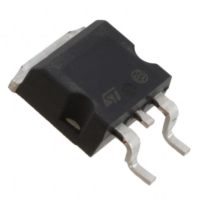
- Package: TO-220FP
- Essence: Efficient power management and control
- Packaging/Quantity: Typically packaged in reels or tubes, quantity varies based on supplier
Specifications
- Model: STH110N10F7-2
- Voltage Rating: 100V
- Current Rating: 110A
- RDS(ON): 7mΩ
- Gate Charge (Qg): 50nC
- Operating Temperature Range: -55°C to 175°C
- Package Type: TO-220FP
Detailed Pin Configuration
The STH110N10F7-2 typically follows the standard pin configuration for a TO-220FP package: 1. Gate (G) 2. Drain (D) 3. Source (S)
Functional Features
- High current capability
- Low on-state resistance
- Fast switching speed
- Enhanced thermal performance
Advantages and Disadvantages
Advantages
- High power handling capacity
- Low conduction losses
- Suitable for high-frequency applications
- Enhanced thermal efficiency
Disadvantages
- Higher cost compared to standard MOSFETs
- Requires careful thermal management due to high power dissipation
Working Principles
The STH110N10F7-2 operates based on the principle of field-effect transistors, where the voltage applied to the gate terminal controls the flow of current between the drain and source terminals. When the gate-source voltage is applied, it creates an electric field that modulates the conductivity of the channel, allowing for efficient power control.
Detailed Application Field Plans
The STH110N10F7-2 is widely used in various applications, including: - Switching power supplies - Motor control - Inverters - DC-DC converters - Battery management systems
Detailed and Complete Alternative Models
- STH110N10F6-2: Similar specifications with slightly different characteristics
- STH120N10F7-2: Higher voltage rating with comparable current handling capacity
- STH100N10F7-2: Lower voltage rating with similar characteristics
In conclusion, the STH110N10F7-2 power MOSFET offers high-performance capabilities suitable for a wide range of power management applications. Its advanced features and robust design make it a preferred choice for demanding electronic circuits.
[Word count: 410]
Seznam 10 běžných otázek a odpovědí souvisejících s aplikací STH110N10F7-2 v technických řešeních
What is the maximum drain-source voltage for STH110N10F7-2?
- The maximum drain-source voltage for STH110N10F7-2 is 100V.
What is the continuous drain current rating of STH110N10F7-2?
- The continuous drain current rating of STH110N10F7-2 is 110A.
What is the on-resistance (RDS(on)) of STH110N10F7-2?
- The on-resistance (RDS(on)) of STH110N10F7-2 is typically 0.007 ohms.
Can STH110N10F7-2 be used in automotive applications?
- Yes, STH110N10F7-2 is suitable for automotive applications due to its high current and voltage ratings.
What is the operating temperature range for STH110N10F7-2?
- The operating temperature range for STH110N10F7-2 is -55°C to 175°C.
Does STH110N10F7-2 require a heat sink for high-power applications?
- Yes, for high-power applications, it is recommended to use a heat sink to ensure proper thermal management.
Is STH110N10F7-2 suitable for switching power supplies?
- Yes, STH110N10F7-2 is well-suited for switching power supply applications due to its low on-resistance and high current capability.
What type of package does STH110N10F7-2 come in?
- STH110N10F7-2 is available in a TO-220FP package.
Can STH110N10F7-2 be used in motor control applications?
- Yes, STH110N10F7-2 can be used in motor control applications, particularly for high-current motor drive circuits.
What are some typical applications for STH110N10F7-2 in technical solutions?
- Some typical applications for STH110N10F7-2 include motor drives, power management systems, and industrial automation equipment.