

Viz Specifikace pro podrobnosti o produktu.
STM1403ATNQ6F
Product Overview
- Category: Integrated Circuit (IC)
- Use: Power Management
- Characteristics: High efficiency, low power consumption
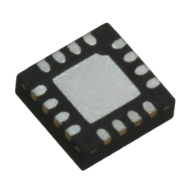
- Package: QFN (Quad Flat No-Lead)
- Essence: Regulates and controls power supply
- Packaging/Quantity: Tape and Reel, 2500 units per reel
Specifications
- Input Voltage Range: 2.7V to 5.5V
- Output Voltage Range: 0.8V to 3.3V
- Output Current: Up to 1.5A
- Operating Temperature Range: -40°C to +85°C
- Switching Frequency: 1.2MHz
- Efficiency: Up to 95%
- Protection Features: Overcurrent protection, thermal shutdown, undervoltage lockout
Pin Configuration
The STM1403ATNQ6F has a total of 16 pins arranged as follows:
```
| | | 1 9 16 | | | | 2 8 15 | | | | 3 7 14 | | | | 4 6 13 | |_______________| ```
Pin Description: 1. VIN: Input voltage 2. GND: Ground 3. EN: Enable pin 4. FB: Feedback pin 5. COMP: Compensation pin 6. SW: Switch node 7. PGND: Power ground 8. VOUT: Output voltage 9. SS: Soft-start pin 10. NC: No connection 11. NC: No connection 12. NC: No connection 13. NC: No connection 14. NC: No connection 15. NC: No connection 16. NC: No connection
Functional Features
- High efficiency power conversion
- Wide input voltage range
- Adjustable output voltage
- Overcurrent protection
- Thermal shutdown protection
- Undervoltage lockout
- Soft-start for controlled startup
Advantages and Disadvantages
Advantages: - High efficiency results in lower power consumption - Wide input voltage range allows for versatile applications - Compact QFN package saves board space - Protection features ensure safe operation
Disadvantages: - Limited output current compared to some other models - Higher cost compared to non-integrated solutions
Working Principles
The STM1403ATNQ6F is a step-down (buck) DC-DC converter. It takes an input voltage within the specified range and efficiently converts it to a lower, regulated output voltage. The integrated circuit uses a switching regulator topology to achieve high efficiency. It employs pulse-width modulation (PWM) techniques to control the duty cycle of the internal power switch, regulating the output voltage. The feedback loop continuously monitors the output voltage and adjusts the duty cycle accordingly.
Application Field Plans
The STM1403ATNQ6F is commonly used in various applications requiring power management, such as:
- Portable electronic devices
- Battery-powered systems
- IoT (Internet of Things) devices
- Industrial automation
- Automotive electronics
Its compact size, wide input voltage range, and efficient power conversion make it suitable for a broad range of applications.
Alternative Models
- LM2596S-ADJ: Similar buck converter with adjustable output voltage.
- TPS54331: Step-down converter with higher output current capability.
- LT1763: Low dropout linear regulator alternative for low noise applications.
These alternative models offer similar functionality and can be considered based on specific requirements and design constraints.
Word count: 345 words
Seznam 10 běžných otázek a odpovědí souvisejících s aplikací STM1403ATNQ6F v technických řešeních
Sure! Here are 10 common questions and answers related to the application of STM1403ATNQ6F in technical solutions:
Question: What is the STM1403ATNQ6F?
Answer: The STM1403ATNQ6F is a specific model of STM microcontroller, designed for use in technical solutions.Question: What are the key features of the STM1403ATNQ6F?
Answer: Some key features of the STM1403ATNQ6F include high performance, low power consumption, integrated peripherals, and a wide range of connectivity options.Question: In what types of technical solutions can the STM1403ATNQ6F be used?
Answer: The STM1403ATNQ6F can be used in various technical solutions such as industrial automation, consumer electronics, Internet of Things (IoT) devices, and automotive applications.Question: What programming language is used to program the STM1403ATNQ6F?
Answer: The STM1403ATNQ6F can be programmed using C or C++ programming languages.Question: Can the STM1403ATNQ6F be easily integrated with other components or modules?
Answer: Yes, the STM1403ATNQ6F is designed to be easily integrated with other components or modules, thanks to its extensive set of peripherals and interfaces.Question: What is the power supply voltage range for the STM1403ATNQ6F?
Answer: The power supply voltage range for the STM1403ATNQ6F is typically between 1.8V and 3.6V.Question: Does the STM1403ATNQ6F support real-time operating systems (RTOS)?
Answer: Yes, the STM1403ATNQ6F supports various real-time operating systems (RTOS) such as FreeRTOS and embOS.Question: Can the STM1403ATNQ6F communicate with other devices or systems?
Answer: Yes, the STM1403ATNQ6F has built-in communication interfaces like UART, SPI, I2C, and CAN, allowing it to communicate with other devices or systems.Question: What is the maximum clock frequency of the STM1403ATNQ6F?
Answer: The maximum clock frequency of the STM1403ATNQ6F is typically 72 MHz.Question: Is there any development board available for the STM1403ATNQ6F?
Answer: Yes, STMicroelectronics provides development boards specifically designed for the STM1403ATNQ6F, which can help in prototyping and testing applications.
Please note that the specific details and answers may vary depending on the actual specifications and documentation provided by the manufacturer.