

Viz Specifikace pro podrobnosti o produktu.
TS271ACDT
Product Overview
- Category: Integrated Circuit (IC)
- Use: Operational Amplifier
- Characteristics: Low-power, Rail-to-Rail Input/Output, Single Supply
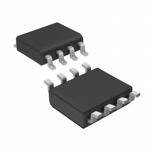
- Package: SOIC-8 (Small Outline Integrated Circuit), Tape and Reel
- Essence: The TS271ACDT is a low-power operational amplifier designed for various applications requiring rail-to-rail input/output capabilities.
- Packaging/Quantity: The TS271ACDT is available in a standard SOIC-8 package and is supplied in tape and reel format.
Specifications
- Supply Voltage: 2.7V to 16V
- Input Offset Voltage: ±1mV (maximum)
- Input Bias Current: ±1pA (typical)
- Gain Bandwidth Product: 3MHz (typical)
- Slew Rate: 1.6V/µs (typical)
- Quiescent Current: 50µA (typical)
- Operating Temperature Range: -40°C to +125°C
Detailed Pin Configuration
The TS271ACDT has a standard SOIC-8 package with the following pin configuration:
```
| | --| IN- VCC |-- --| IN+ OUT |-- --| GND NC |-- |___________| ```
Pin Description: - IN-: Inverting Input - IN+: Non-Inverting Input - OUT: Output - VCC: Positive Supply Voltage - GND: Ground - NC: No Connection
Functional Features
- Rail-to-Rail Input/Output: The TS271ACDT can accept and provide signals that are close to its supply voltage range, allowing for maximum dynamic range.
- Low Power Consumption: With a quiescent current of only 50µA, the TS271ACDT is suitable for battery-powered applications.
- Wide Supply Voltage Range: The operational amplifier can operate from 2.7V to 16V, providing flexibility in various voltage supply scenarios.
Advantages and Disadvantages
Advantages: - Rail-to-rail input/output capabilities - Low power consumption - Wide supply voltage range
Disadvantages: - Limited gain bandwidth product compared to some other operational amplifiers - Higher input offset voltage compared to precision amplifiers
Working Principles
The TS271ACDT is based on a CMOS (Complementary Metal-Oxide-Semiconductor) technology, which allows for low-power operation and rail-to-rail input/output characteristics. It utilizes internal circuitry to amplify and process input signals according to the specified gain and output characteristics.
Detailed Application Field Plans
The TS271ACDT is suitable for a wide range of applications, including but not limited to: 1. Battery-powered devices 2. Sensor signal conditioning 3. Portable audio equipment 4. Signal amplification in low-voltage systems 5. Industrial control systems
Detailed and Complete Alternative Models
- LM324: Quad Operational Amplifier with similar specifications and package options.
- MCP6001: Single Operational Amplifier with rail-to-rail input/output and low-power characteristics.
- TLV2462: Dual Operational Amplifier with rail-to-rail input/output and low-power consumption.
These alternative models offer similar functionality and can be considered as substitutes for the TS271ACDT depending on specific requirements and availability.
Word count: 400 words
Seznam 10 běžných otázek a odpovědí souvisejících s aplikací TS271ACDT v technických řešeních
Sure! Here are 10 common questions and answers related to the application of TS271ACDT in technical solutions:
Q: What is TS271ACDT? A: TS271ACDT is a specific model of operational amplifier (op-amp) commonly used in various technical solutions.
Q: What are the key features of TS271ACDT? A: The key features of TS271ACDT include low input offset voltage, low input bias current, high slew rate, and wide bandwidth.
Q: In what applications can TS271ACDT be used? A: TS271ACDT can be used in a wide range of applications such as signal conditioning, audio amplification, active filters, and instrumentation.
Q: What is the supply voltage range for TS271ACDT? A: The supply voltage range for TS271ACDT typically ranges from ±2V to ±18V.
Q: What is the input offset voltage of TS271ACDT? A: The input offset voltage of TS271ACDT is typically very low, around a few microvolts.
Q: Can TS271ACDT operate in single-supply configurations? A: Yes, TS271ACDT can operate in both dual-supply and single-supply configurations, making it versatile for different applications.
Q: What is the maximum output current of TS271ACDT? A: The maximum output current of TS271ACDT is typically around 20mA.
Q: Is TS271ACDT suitable for precision applications? A: Yes, TS271ACDT is suitable for precision applications due to its low input offset voltage and low input bias current.
Q: Does TS271ACDT have built-in protection features? A: Yes, TS271ACDT typically includes built-in protection features such as short-circuit protection and thermal shutdown.
Q: Can TS271ACDT be used in high-frequency applications? A: Yes, TS271ACDT has a wide bandwidth and high slew rate, making it suitable for high-frequency applications up to several megahertz.
Please note that the specific details and specifications may vary depending on the manufacturer and datasheet of TS271ACDT.