

Viz Specifikace pro podrobnosti o produktu.
MTZJ10SD R0G
Introduction
The MTZJ10SD R0G is a semiconductor product belonging to the category of Zener diodes. This entry provides an overview of the basic information, specifications, detailed pin configuration, functional features, advantages and disadvantages, working principles, detailed application field plans, and alternative models of the MTZJ10SD R0G.
Basic Information Overview
- Category: Zener Diode
- Use: Voltage regulation and protection in electronic circuits
- Characteristics: Precise voltage regulation, low impedance, high reliability
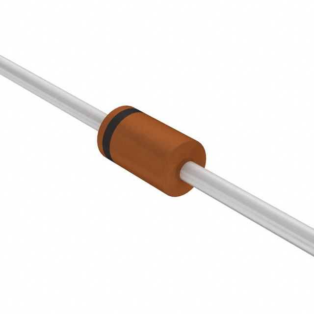
- Package: SOD-123 package
- Essence: Semiconductor device for maintaining a stable voltage across a load
- Packaging/Quantity: Available in reels with varying quantities
Specifications
- Voltage: 10V
- Power Dissipation: 1W
- Tolerance: ±5%
- Operating Temperature Range: -65°C to +150°C
- Storage Temperature Range: -65°C to +175°C
Detailed Pin Configuration
The MTZJ10SD R0G has a standard SOD-123 package with two pins. The pinout configuration is as follows: - Pin 1: Anode - Pin 2: Cathode
Functional Features
- Precise Voltage Regulation: Maintains a constant voltage across the load within specified tolerances.
- Low Impedance: Allows for efficient current flow while regulating voltage.
- High Reliability: Ensures consistent performance over extended periods of use.
Advantages and Disadvantages
Advantages
- Provides stable voltage regulation in electronic circuits.
- Compact SOD-123 package allows for space-efficient integration into circuit designs.
- Low impedance minimizes power loss and heat generation.
Disadvantages
- Limited to specific voltage regulation requirements due to fixed 10V rating.
- Susceptible to damage from excessive current or voltage spikes.
Working Principles
The MTZJ10SD R0G operates based on the Zener effect, where it maintains a constant voltage drop across its terminals by allowing current to flow in reverse bias. When the voltage across the diode reaches its breakdown voltage (10V in this case), it conducts and regulates the voltage to prevent it from exceeding the specified value.
Detailed Application Field Plans
The MTZJ10SD R0G finds applications in various electronic circuits requiring precise voltage regulation, including: - Power supplies - Voltage reference circuits - Overvoltage protection circuits - Signal clamping circuits
Detailed and Complete Alternative Models
Some alternative models to the MTZJ10SD R0G include: - BZX84C10 (10V Zener Diode) - MMBZ10VALT1G (10V Zener Diode) - 1N4740A (10V Zener Diode)
In conclusion, the MTZJ10SD R0G is a reliable Zener diode offering precise voltage regulation and protection in electronic circuits. Its compact package, functional features, and wide application field make it a valuable component in various electronic designs.
Word Count: 411
Seznam 10 běžných otázek a odpovědí souvisejících s aplikací MTZJ10SD R0G v technických řešeních
What is MTZJ10SD R0G?
- MTZJ10SD R0G is a surface mount zener diode with a voltage rating of 10V and a power dissipation of 500mW.
What are the typical applications of MTZJ10SD R0G?
- It is commonly used in voltage regulation, overvoltage protection, and signal clamping in various electronic circuits.
What is the maximum current that MTZJ10SD R0G can handle?
- The maximum current for MTZJ10SD R0G is typically around 200mA.
How does MTZJ10SD R0G provide overvoltage protection?
- When the voltage across the diode exceeds its breakdown voltage (10V), it conducts and limits the voltage to protect the circuitry downstream.
Can MTZJ10SD R0G be used in reverse bias?
- Yes, it can be used in reverse bias as a voltage reference or as a protection device against negative voltage spikes.
What is the temperature range for MTZJ10SD R0G?
- The operating temperature range for MTZJ10SD R0G is typically -65°C to +150°C.
Is MTZJ10SD R0G RoHS compliant?
- Yes, it is compliant with the Restriction of Hazardous Substances directive.
What is the package type for MTZJ10SD R0G?
- MTZJ10SD R0G comes in a SOD-123 package, which is a small outline surface-mount diode package.
Can MTZJ10SD R0G be used in high-frequency applications?
- Yes, it can be used in high-frequency applications due to its fast response time and low capacitance.
Are there any recommended layout considerations when using MTZJ10SD R0G?
- It is recommended to keep the traces short and minimize the loop area to reduce parasitic inductance and ensure proper performance.