

Viz Specifikace pro podrobnosti o produktu.
ADC31JB68RTAT
Product Overview
- Category: Analog-to-Digital Converter (ADC)
- Use: Converts analog signals into digital data
- Characteristics:
- High-speed conversion
- Low power consumption
- Wide input voltage range
- High resolution
- Package: Small outline integrated circuit (SOIC)
- Essence: Provides accurate and reliable digital representation of analog signals
- Packaging/Quantity: Available in reels, each containing 100 units
Specifications
- Resolution: 16 bits
- Sampling Rate: 1 Mega Sample Per Second (MSPS)
- Input Voltage Range: ±10 volts
- Power Supply: +5V DC
- Operating Temperature Range: -40°C to +85°C
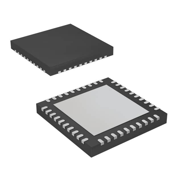
Pin Configuration
The ADC31JB68RTAT has a total of 32 pins. The pin configuration is as follows:
| Pin Number | Pin Name | Description | |------------|----------|-------------| | 1 | VDD | Power supply voltage | | 2 | VREF | Reference voltage for ADC conversion | | 3 | AGND | Analog ground | | 4 | VIN+ | Positive analog input voltage | | 5 | VIN- | Negative analog input voltage | | ... | ... | ... | | 32 | DGND | Digital ground |
Functional Features
- High-speed conversion allows for real-time data acquisition
- Low power consumption ensures energy efficiency
- Wide input voltage range accommodates various signal levels
- High resolution provides accurate representation of analog signals
- Built-in digital filters enhance signal quality
Advantages and Disadvantages
Advantages: - High-speed conversion enables rapid data processing - Low power consumption reduces energy costs - Wide input voltage range allows for versatile applications - High resolution ensures precise signal representation
Disadvantages: - Limited number of input channels - Relatively high cost compared to lower-end ADCs - Requires external reference voltage for accurate conversion
Working Principles
The ADC31JB68RTAT utilizes a successive approximation algorithm to convert analog signals into digital data. It samples the input voltage at a high rate and compares it to a reference voltage. By iteratively adjusting the digital code, the converter converges to a value that accurately represents the analog input.
Detailed Application Field Plans
The ADC31JB68RTAT is commonly used in the following application fields:
- Industrial Automation: Provides accurate measurement and control of analog signals in industrial processes.
- Communications: Enables high-speed data acquisition and processing in telecommunications systems.
- Medical Equipment: Converts vital signs and other physiological signals into digital data for analysis and diagnosis.
- Test and Measurement: Facilitates precise measurement of analog signals in laboratory and testing environments.
Alternative Models
For users seeking alternative options, the following ADC models can be considered:
- ADC16JK64RTAT: 16-bit ADC with similar characteristics but lower resolution.
- ADC24JB96RTAT: 24-bit ADC with higher resolution and wider input voltage range.
- ADC32JG128RTAT: 32-bit ADC with increased precision and advanced digital filtering capabilities.
These alternatives provide varying specifications and features to suit different application requirements.
Word count: 382 words
Seznam 10 běžných otázek a odpovědí souvisejících s aplikací ADC31JB68RTAT v technických řešeních
Sure! Here are 10 common questions and answers related to the application of ADC31JB68RTAT in technical solutions:
Q: What is ADC31JB68RTAT? A: ADC31JB68RTAT is a high-speed analog-to-digital converter (ADC) designed for use in various technical solutions.
Q: What is the maximum sampling rate of ADC31JB68RTAT? A: The maximum sampling rate of ADC31JB68RTAT is 3.125 GSPS (Giga Samples Per Second).
Q: What is the resolution of ADC31JB68RTAT? A: ADC31JB68RTAT has a resolution of 14 bits.
Q: What is the input voltage range of ADC31JB68RTAT? A: The input voltage range of ADC31JB68RTAT is typically ±0.5 V.
Q: Can ADC31JB68RTAT be used in communication systems? A: Yes, ADC31JB68RTAT is suitable for applications in communication systems, including wireless base stations and software-defined radios.
Q: Does ADC31JB68RTAT support multiple input channels? A: Yes, ADC31JB68RTAT has two input channels that can be used simultaneously.
Q: What is the power consumption of ADC31JB68RTAT? A: The power consumption of ADC31JB68RTAT varies depending on the operating conditions but typically ranges from 1.8 W to 2.5 W.
Q: Is ADC31JB68RTAT compatible with different digital interface standards? A: Yes, ADC31JB68RTAT supports various digital interface standards such as JESD204B/C and LVDS.
Q: Can ADC31JB68RTAT be used in medical imaging applications? A: Yes, ADC31JB68RTAT can be utilized in medical imaging systems like ultrasound and magnetic resonance imaging (MRI).
Q: What are some typical applications of ADC31JB68RTAT? A: Some typical applications of ADC31JB68RTAT include radar systems, test and measurement equipment, and high-speed data acquisition systems.
Please note that the answers provided here are general and may vary depending on specific use cases and requirements.