

Viz Specifikace pro podrobnosti o produktu.
ADS5103CPFBRG4
Product Overview
- Category: Integrated Circuit
- Use: Analog-to-Digital Converter (ADC)
- Characteristics: High-speed, low-power, precision ADC
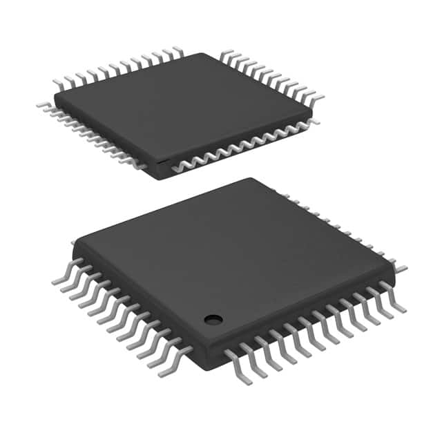
- Package: 48-pin LQFP
- Essence: Converts analog signals into digital data
- Packaging/Quantity: Tape and reel, 250 units per reel
Specifications
- Resolution: 12 bits
- Sampling Rate: 100 MSPS (Mega Samples Per Second)
- Input Voltage Range: 0 to 2.5 V
- Power Supply: 3.3 V
- Operating Temperature Range: -40°C to +85°C
- Differential Non-Linearity (DNL): ±0.5 LSB (Least Significant Bit)
- Integral Non-Linearity (INL): ±1 LSB
- Signal-to-Noise Ratio (SNR): 70 dB
- Total Harmonic Distortion (THD): -80 dB
Pin Configuration
The ADS5103CPFBRG4 has a total of 48 pins. The pin configuration is as follows:
- VREFP: Positive reference voltage input
- VREFN: Negative reference voltage input
- AGND: Analog ground
- VINP: Positive analog input
- VCM: Common-mode voltage output
- VINN: Negative analog input
- CLKOUT: Clock output
- CLKIN: Clock input
- DGND: Digital ground
- D[11:0]: Digital output bits
- PDWN: Power-down control input
- RESET: Reset control input
- CS: Chip select input
- SCLK: Serial clock input
- SDATA: Serial data input/output
- DVDD: Digital power supply
(Continues for the remaining pins...)
Functional Features
- High-speed conversion with a sampling rate of 100 MSPS
- Low power consumption for energy-efficient operation
- Precise analog-to-digital conversion with 12-bit resolution
- Wide input voltage range of 0 to 2.5 V
- Excellent linearity with low differential and integral non-linearity
- Good signal-to-noise ratio and low harmonic distortion
Advantages and Disadvantages
Advantages: - High-speed and accurate conversion - Low power consumption - Wide input voltage range - Good linearity and signal quality
Disadvantages: - Limited resolution compared to higher-end ADCs - Requires external clock source for operation
Working Principles
The ADS5103CPFBRG4 is an analog-to-digital converter that converts continuous analog signals into discrete digital data. It utilizes a high-speed sampling technique to capture the analog input signal and then quantizes it into digital values using its internal circuitry. The converted digital data can then be processed by a microcontroller or other digital devices.
Detailed Application Field Plans
The ADS5103CPFBRG4 is commonly used in various applications that require high-speed and precise analog-to-digital conversion. Some of the typical application fields include:
- Communications: Used in wireless communication systems for signal processing and modulation/demodulation.
- Test and Measurement: Employed in oscilloscopes, spectrum analyzers, and data acquisition systems for accurate signal analysis.
- Medical Imaging: Utilized in medical imaging equipment such as ultrasound machines and MRI scanners for digitizing analog signals.
- Industrial Automation: Integrated into industrial control systems for monitoring and controlling analog signals in real-time.
- Audio Processing: Found in audio equipment like mixers, amplifiers, and digital audio workstations for converting analog audio signals into digital format.
Detailed and Complete Alternative Models
- ADS8860: 16-bit, 1 MSPS ADC with SPI interface
- ADS124S08: 24-bit, 4-channel, low-power ADC with PGA and SPI interface
- ADS1278: 24-bit, 8-channel, high-speed ADC with simultaneous sampling capability
- ADS1015: 12-bit, 4-channel, I2C-compatible ADC with programmable gain amplifier
- ADS1286: 24-bit, 6-channel, delta-sigma ADC with integrated PGA and temperature sensor
(Note: This is not an exhaustive list of alternative models. Please refer to the manufacturer's documentation for a complete list.)
Word Count: 550
Seznam 10 běžných otázek a odpovědí souvisejících s aplikací ADS5103CPFBRG4 v technických řešeních
Sure! Here are 10 common questions and answers related to the application of ADS5103CPFBRG4 in technical solutions:
Q: What is the ADS5103CPFBRG4? A: The ADS5103CPFBRG4 is a high-speed differential amplifier designed for applications requiring wide bandwidth, low distortion, and low noise.
Q: What are the key features of the ADS5103CPFBRG4? A: The key features include a bandwidth of up to 1 GHz, low input voltage noise, low distortion, high common-mode rejection ratio (CMRR), and a wide supply voltage range.
Q: What are some typical applications of the ADS5103CPFBRG4? A: The ADS5103CPFBRG4 is commonly used in applications such as communications systems, test and measurement equipment, medical imaging, and high-speed data acquisition.
Q: How does the ADS5103CPFBRG4 achieve low distortion? A: The ADS5103CPFBRG4 utilizes a high-gain, low-noise architecture along with advanced design techniques to minimize distortion and provide accurate amplification of signals.
Q: Can the ADS5103CPFBRG4 operate on a single power supply? A: No, the ADS5103CPFBRG4 requires dual power supplies, typically ±5V to ±15V, to operate properly.
Q: What is the maximum differential input voltage that the ADS5103CPFBRG4 can handle? A: The ADS5103CPFBRG4 can handle a maximum differential input voltage of ±2V.
Q: Does the ADS5103CPFBRG4 have built-in protection features? A: Yes, the ADS5103CPFBRG4 includes built-in protection against overvoltage, overcurrent, and thermal shutdown to ensure safe operation.
Q: What is the output voltage swing of the ADS5103CPFBRG4? A: The ADS5103CPFBRG4 has a typical output voltage swing of ±2V when operating on a ±5V power supply.
Q: Can the ADS5103CPFBRG4 be used in high-frequency applications? A: Yes, the ADS5103CPFBRG4 has a wide bandwidth of up to 1 GHz, making it suitable for high-frequency applications.
Q: Is there any evaluation board available for the ADS5103CPFBRG4? A: Yes, Texas Instruments provides an evaluation board (EVM) for the ADS5103CPFBRG4, which allows users to easily test and evaluate its performance in their specific applications.
Please note that these answers are general and may vary depending on the specific requirements and use cases of your technical solution.