

Viz Specifikace pro podrobnosti o produktu.
ADS54J20IRMP
Product Overview
Category
The ADS54J20IRMP belongs to the category of analog-to-digital converters (ADCs).
Use
This product is primarily used for converting analog signals into digital data in various applications.
Characteristics
- High-speed conversion: The ADS54J20IRMP offers fast and accurate analog-to-digital conversion.
- High resolution: It provides high-resolution digitization, ensuring precise signal capture.
- Low power consumption: This ADC is designed to operate efficiently with minimal power consumption.
- Wide input range: The device can handle a wide range of input voltages, making it versatile for different applications.
Package
The ADS54J20IRMP comes in a compact and robust package, ensuring durability and ease of integration into electronic systems.
Essence
The essence of the ADS54J20IRMP lies in its ability to convert analog signals into digital format with high speed, accuracy, and efficiency.
Packaging/Quantity
This product is typically packaged individually and is available in various quantities depending on customer requirements.
Specifications
- Resolution: 16 bits
- Sampling Rate: Up to 1 GSPS (Giga Samples Per Second)
- Input Voltage Range: ±2 V
- Power Supply: 3.3 V
- Operating Temperature Range: -40°C to +85°C
- Interface: Serial LVDS (Low-Voltage Differential Signaling)
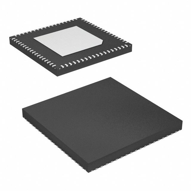
Detailed Pin Configuration
The ADS54J20IRMP has a total of 64 pins. Here is a brief overview of some key pins:
- VDD: Power supply pin (+3.3 V)
- VREFP/VREFN: Reference voltage pins for positive and negative inputs
- VINP/VINN: Analog input pins
- CLKP/CLKN: Clock input pins
- D[0:15]: Digital output pins
- RESET: Reset pin for device initialization
For a complete pin configuration diagram, please refer to the product datasheet.
Functional Features
- High-speed data conversion with low latency
- Programmable gain amplifier (PGA) for signal conditioning
- Digital down-conversion (DDC) for frequency translation
- Built-in digital filters for noise reduction
- Flexible input/output configurations for versatile applications
Advantages and Disadvantages
Advantages
- High-resolution digitization for accurate signal capture
- Fast conversion speed enables real-time processing
- Low power consumption for energy-efficient operation
- Wide input voltage range accommodates various signal levels
- Compact package for easy integration into electronic systems
Disadvantages
- Requires external components for proper operation
- Limited to serial LVDS interface
- Higher cost compared to lower-end ADCs
Working Principles
The ADS54J20IRMP operates based on the principle of sampling and quantization. It samples the analog input signal at a high rate and converts each sample into a digital value using its internal circuitry. The resulting digital data can then be processed by a microcontroller or other digital devices.
Detailed Application Field Plans
The ADS54J20IRMP finds application in various fields, including:
- Communications: Used in wireless communication systems for signal processing and baseband applications.
- Test and Measurement: Enables high-precision measurements in scientific instruments and test equipment.
- Radar Systems: Provides accurate digitization of radar signals for target detection and tracking.
- Medical Imaging: Used in medical imaging devices for capturing and processing analog signals from sensors.
- Industrial Automation: Enables precise control and monitoring in industrial automation systems.
Detailed and Complete Alternative Models
- ADS54J40IRMP: Similar to ADS54J20IRMP but with higher resolution (24 bits).
- ADS54J10IRMP: Lower-cost alternative with slightly reduced performance specifications.
- ADS54J60IRMP: Higher-end model with increased sampling rate (up to 2 GSPS).
These alternative models offer different features and specifications to cater to specific application requirements.
Word count: 550 words
Seznam 10 běžných otázek a odpovědí souvisejících s aplikací ADS54J20IRMP v technických řešeních
Sure! Here are 10 common questions and answers related to the application of ADS54J20IRMP in technical solutions:
Q: What is the ADS54J20IRMP? A: The ADS54J20IRMP is a high-performance analog-to-digital converter (ADC) manufactured by Texas Instruments.
Q: What is the resolution of the ADS54J20IRMP? A: The ADS54J20IRMP has a resolution of 14 bits, meaning it can represent analog signals with 2^14 (16,384) discrete levels.
Q: What is the sampling rate of the ADS54J20IRMP? A: The ADS54J20IRMP has a maximum sampling rate of 500 Mega-samples per second (MSPS), allowing it to capture high-frequency signals accurately.
Q: What is the input voltage range of the ADS54J20IRMP? A: The ADS54J20IRMP has a differential input voltage range of ±2 V, which can be useful for a wide range of applications.
Q: Does the ADS54J20IRMP support multiple input channels? A: Yes, the ADS54J20IRMP supports dual-channel operation, allowing simultaneous sampling of two different analog signals.
Q: What is the power supply requirement for the ADS54J20IRMP? A: The ADS54J20IRMP requires a single 1.8 V power supply for its core operation and a separate 3.3 V supply for its digital interface.
Q: Can the ADS54J20IRMP be used in low-power applications? A: Yes, the ADS54J20IRMP features a power-down mode that reduces its power consumption when not actively converting analog signals.
Q: What is the interface used to communicate with the ADS54J20IRMP? A: The ADS54J20IRMP uses a JESD204B serial interface, which allows for high-speed data transfer and synchronization with other devices.
Q: Are there any evaluation modules available for the ADS54J20IRMP? A: Yes, Texas Instruments provides an evaluation module (EVM) for the ADS54J20IRMP, which can help users quickly prototype and test their designs.
Q: What are some typical applications of the ADS54J20IRMP? A: The ADS54J20IRMP is commonly used in applications such as wireless communication systems, radar systems, medical imaging, and test and measurement equipment.
Please note that these answers are general and may vary depending on specific requirements and use cases.