

Viz Specifikace pro podrobnosti o produktu.
ADS8694IDBT
Product Overview
Category: Analog-to-Digital Converter (ADC)
Use: The ADS8694IDBT is a high-performance, 16-bit ADC designed for precision measurement applications. It offers exceptional accuracy and speed, making it suitable for a wide range of industrial and scientific applications.
Characteristics: - High resolution: 16-bit resolution provides precise measurement capabilities. - Fast conversion rate: The ADC can perform conversions at a rate of up to 1 MSPS (Mega Samples Per Second). - Low power consumption: The device operates at low power levels, making it suitable for battery-powered applications. - Wide input voltage range: The ADC can accept input voltages from -5V to +5V, allowing for versatile signal acquisition. - Integrated features: The device includes built-in reference voltage, temperature sensor, and programmable gain amplifier.
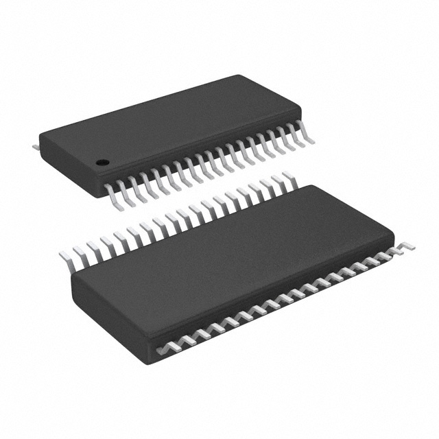
Package: The ADS8694IDBT is available in a compact and industry-standard TSSOP-38 package, which ensures easy integration into various circuit designs.
Essence: The essence of the ADS8694IDBT lies in its ability to provide accurate and high-resolution analog-to-digital conversion, enabling precise measurement and control in diverse applications.
Packaging/Quantity: The ADS8694IDBT is typically sold in reels containing 250 units per reel.
Specifications
- Resolution: 16 bits
- Conversion Rate: Up to 1 MSPS
- Input Voltage Range: -5V to +5V
- Power Supply: 3.3V
- Operating Temperature Range: -40°C to +85°C
- Package Type: TSSOP-38
Detailed Pin Configuration
The ADS8694IDBT has a total of 38 pins. Below is the detailed pin configuration:

Functional Features
- High-resolution conversion: The 16-bit resolution ensures accurate measurement of analog signals.
- Fast conversion rate: The ADC can perform conversions at a rate of up to 1 MSPS, enabling real-time data acquisition.
- Integrated features: Built-in reference voltage, temperature sensor, and programmable gain amplifier enhance the functionality and flexibility of the device.
- Low power consumption: The ADC operates at low power levels, making it suitable for power-constrained applications.
- SPI interface: The device supports Serial Peripheral Interface (SPI) for easy communication with microcontrollers or other digital devices.
Advantages and Disadvantages
Advantages: - High resolution for precise measurements - Fast conversion rate enables real-time data acquisition - Integrated features reduce external component count - Low power consumption extends battery life - Wide input voltage range allows versatile signal acquisition
Disadvantages: - Limited to 16-bit resolution, may not be suitable for applications requiring higher precision - Requires external microcontroller or digital device for control and data processing
Working Principles
The ADS8694IDBT utilizes a successive approximation register (SAR) architecture to convert analog signals into digital data. It samples the input voltage, compares it against an internal reference voltage, and iteratively determines the digital representation of the analog signal. The built-in programmable gain amplifier allows for signal amplification or attenuation, enhancing the dynamic range of the ADC.
Detailed Application Field Plans
The ADS8694IDBT finds applications in various fields that require high-precision analog-to-digital conversion. Some potential application areas include:
Industrial Automation: The ADC can be used in industrial control systems, process monitoring, and instrumentation to accurately measure and control analog signals.
Medical Equipment: The high resolution and accuracy of the ADC make it suitable for medical devices such as patient monitoring systems, diagnostic equipment, and laboratory instruments.
Test and Measurement: The ADC can be utilized in test and measurement equipment, data acquisition systems, and scientific research applications that require precise analog signal conversion.
Energy Management: The device can be employed in energy monitoring systems, smart grid applications, and renewable energy systems to measure and monitor voltage and current signals accurately.
Detailed and Complete Alternative Models
ADS8684IDBT: Similar to the ADS8694IDBT, this 16-bit ADC offers high-resolution conversion and fast conversion rate. It comes in a TSSOP-38 package and is suitable for precision measurement applications.
ADS8674IDBT: This 16-bit ADC also provides high-resolution conversion and features a low power consumption design. It is available in a TSSOP-38 package and is ideal for battery-powered applications.
ADS8884IDBT: Offering 18-bit resolution, this ADC provides even higher precision than the ADS8694IDBT. It operates at a slower conversion rate of 500 kSPS (kilo Samples Per Second) but maintains similar characteristics and package type.
ADS7864ID
Seznam 10 běžných otázek a odpovědí souvisejících s aplikací ADS8694IDBT v technických řešeních
Sure! Here are 10 common questions and answers related to the application of ADS8694IDBT in technical solutions:
Q: What is ADS8694IDBT? A: ADS8694IDBT is a high-performance, 16-bit analog-to-digital converter (ADC) from Texas Instruments.
Q: What is the operating voltage range of ADS8694IDBT? A: The operating voltage range of ADS8694IDBT is typically between 2.7V and 5.5V.
Q: What is the maximum sampling rate of ADS8694IDBT? A: ADS8694IDBT has a maximum sampling rate of 500 kilosamples per second (ksps).
Q: What is the resolution of ADS8694IDBT? A: ADS8694IDBT has a resolution of 16 bits, allowing for high-precision measurements.
Q: Can ADS8694IDBT be used in industrial applications? A: Yes, ADS8694IDBT is suitable for various industrial applications such as process control, data acquisition, and instrumentation.
Q: Does ADS8694IDBT support differential inputs? A: Yes, ADS8694IDBT supports both differential and single-ended inputs, providing flexibility in signal conditioning.
Q: What is the input voltage range of ADS8694IDBT? A: The input voltage range of ADS8694IDBT is typically ±VREF, where VREF is the reference voltage provided externally.
Q: Can ADS8694IDBT operate in a low-power mode? A: Yes, ADS8694IDBT features a low-power mode that reduces power consumption when not actively sampling.
Q: Does ADS8694IDBT have built-in digital filters? A: Yes, ADS8694IDBT includes a programmable digital filter that can be configured to meet specific application requirements.
Q: What interface does ADS8694IDBT use for communication? A: ADS8694IDBT utilizes a serial peripheral interface (SPI) for communication with microcontrollers or other digital devices.
Please note that these answers are general and may vary depending on the specific implementation and configuration of ADS8694IDBT in a technical solution.