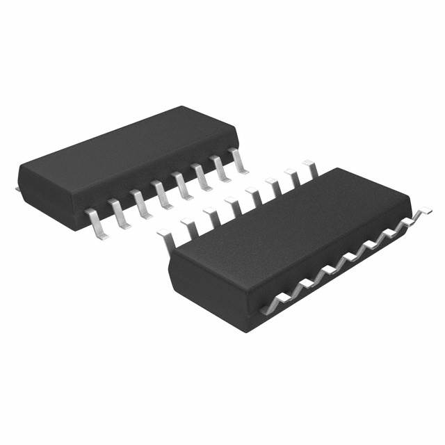
Viz Specifikace pro podrobnosti o produktu.

CD4512BNSR
Product Overview
Category
CD4512BNSR belongs to the category of integrated circuits (ICs).
Use
This IC is commonly used in digital electronics and microcontroller-based systems for various applications.
Characteristics
- CD4512BNSR is a 8-channel multiplexer with latch.
- It operates on a wide voltage range, typically from 3V to 18V.
- The IC has low power consumption and high noise immunity.
- It is designed to be compatible with both TTL and CMOS logic levels.
Package
CD4512BNSR is available in a small outline package (SOIC) with 16 pins.
Essence
The essence of CD4512BNSR lies in its ability to select one out of eight input signals and route it to the output based on the control inputs.
Packaging/Quantity
The IC is typically sold in reels or tubes containing multiple units. The exact quantity may vary depending on the supplier.
Specifications
- Supply Voltage Range: 3V to 18V
- Input Voltage Range: 0V to VDD
- Output Voltage Range: 0V to VDD
- Maximum Operating Frequency: 5MHz
- Maximum Propagation Delay: 250ns
- Operating Temperature Range: -40°C to +85°C
Detailed Pin Configuration
The CD4512BNSR IC has the following pin configuration:
- A0: Channel selection input
- A1: Channel selection input
- A2: Channel selection input
- E: Enable input
- D: Data input
- Q0: Output for channel 0
- Q1: Output for channel 1
- Q2: Output for channel 2
- Q3: Output for channel 3
- Q4: Output for channel 4
- Q5: Output for channel 5
- Q6: Output for channel 6
- Q7: Output for channel 7
- VSS: Ground (0V)
- VDD: Supply voltage
- NC: No connection
Functional Features
- CD4512BNSR is an 8-channel multiplexer with latch functionality.
- It allows the selection of one input channel out of eight using the control inputs A0, A1, and A2.
- The selected input is latched and routed to the corresponding output pin.
- The enable input (E) controls the operation of the IC.
Advantages and Disadvantages
Advantages
- Wide operating voltage range allows compatibility with various systems.
- Low power consumption makes it suitable for battery-powered applications.
- High noise immunity ensures reliable operation in noisy environments.
- Compact SOIC package enables space-saving PCB designs.
Disadvantages
- Limited number of input channels (8) may not be sufficient for certain applications requiring more inputs.
- Propagation delay of 250ns may introduce timing constraints in high-speed applications.
Working Principles
CD4512BNSR operates based on the principle of digital multiplexing. It uses the control inputs (A0, A1, and A2) to select one out of eight input channels. The selected input is then latched and routed to the corresponding output pin. The enable input (E) controls the overall operation of the IC.
Detailed Application Field Plans
CD4512BNSR finds applications in various fields, including but not limited to: - Digital data routing and selection - Microcontroller-based systems - Industrial automation - Communication systems - Consumer electronics
Detailed and Complete Alternative Models
Some alternative models that can be considered as alternatives to CD4512BNSR are: - CD4051B: 8-channel analog multiplexer/demultiplexer - CD74HC4067: 16-channel analog multiplexer/demultiplexer - CD4052B: Dual 4-channel analog multiplexer/demultiplexer
These alternative models offer similar functionality and can be used as substitutes depending on specific requirements.
Word count: 529 words
Seznam 10 běžných otázek a odpovědí souvisejících s aplikací CD4512BNSR v technických řešeních
Sure! Here are 10 common questions and answers related to the application of CD4512BNSR in technical solutions:
Q: What is CD4512BNSR? A: CD4512BNSR is a 8-channel multiplexer/demultiplexer integrated circuit (IC) commonly used in digital electronics.
Q: What is the purpose of CD4512BNSR? A: The purpose of CD4512BNSR is to select one of eight input signals and route it to an output based on the control inputs.
Q: How does CD4512BNSR work? A: CD4512BNSR has three control inputs, which determine the channel selection. The selected input is then routed to the output pin.
Q: What is the voltage range supported by CD4512BNSR? A: CD4512BNSR supports a wide voltage range from 3V to 18V, making it compatible with various power supply systems.
Q: Can CD4512BNSR be used for both analog and digital signals? A: No, CD4512BNSR is designed for digital signals only. It is not suitable for handling analog signals.
Q: What is the maximum frequency at which CD4512BNSR can operate? A: CD4512BNSR can operate at frequencies up to 5 MHz, making it suitable for many digital applications.
Q: Can CD4512BNSR be cascaded to increase the number of channels? A: Yes, multiple CD4512BNSR ICs can be cascaded together to increase the number of channels available.
Q: Does CD4512BNSR have any built-in protection features? A: CD4512BNSR has built-in diode protection on all inputs and outputs, which helps prevent damage from voltage spikes.
Q: Can CD4512BNSR be used in battery-powered applications? A: Yes, CD4512BNSR has a low power consumption and can be used in battery-powered applications effectively.
Q: Are there any specific precautions to consider when using CD4512BNSR? A: It is important to ensure that the voltage levels of the input signals are within the specified range to avoid damaging the IC. Additionally, proper decoupling capacitors should be used for stable operation.
Please note that these answers are general and may vary depending on the specific application and requirements.

