

Viz Specifikace pro podrobnosti o produktu.
CD74HC4514EG4
Product Overview
- Category: Integrated Circuit
- Use: Decoding and demultiplexing 4-to-16 line
- Characteristics: High-speed CMOS logic, low power consumption
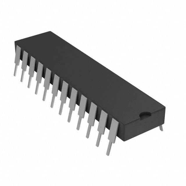
- Package: TSSOP-24
- Essence: CD74HC4514EG4 is a high-speed CMOS logic integrated circuit that is commonly used for decoding and demultiplexing 4-to-16 line. It offers low power consumption and is packaged in a TSSOP-24 package.
Specifications
- Supply Voltage: 2V to 6V
- Input Voltage: 0V to VCC
- Output Voltage: 0V to VCC
- Operating Temperature: -40°C to +85°C
- Propagation Delay: 20ns (typical)
- Output Current: ±25mA
Pin Configuration
The CD74HC4514EG4 has a total of 24 pins. The pin configuration is as follows:
- GND
- A0
- A1
- A2
- A3
- A4
- A5
- A6
- A7
- A8
- A9
- A10
- A11
- A12
- A13
- A14
- A15
- E
- D0
- D1
- D2
- D3
- VCC
Functional Features
- Decodes and demultiplexes 4-to-16 line
- High-speed CMOS logic
- Low power consumption
- Wide operating voltage range
- Schmitt-trigger inputs for noise immunity
- Latch-up performance exceeds 250mA per JESD 17
Advantages and Disadvantages
Advantages
- High-speed operation allows for quick decoding and demultiplexing
- Low power consumption helps in reducing overall energy usage
- Wide operating voltage range provides flexibility in various applications
- Schmitt-trigger inputs ensure reliable operation even in noisy environments
- Latch-up performance exceeds industry standards, ensuring robustness
Disadvantages
- Limited to 4-to-16 line decoding and demultiplexing
- May require additional components for complex applications
Working Principles
The CD74HC4514EG4 works by taking a 4-bit binary input and decoding it into one of the 16 output lines. The enable pin (E) controls the operation of the decoder. When E is high, the decoder is enabled, and the selected output line corresponds to the binary input. When E is low, all output lines are disabled.
Application Field Plans
The CD74HC4514EG4 can be used in various applications that require decoding and demultiplexing of 4-to-16 line. Some potential application fields include:
- Address decoding in microcontrollers and microprocessors
- Data routing in multiplexers and data selectors
- LED matrix control in display systems
- Memory address decoding in memory modules
- Signal routing in communication systems
Alternative Models
Here are some alternative models that offer similar functionality to the CD74HC4514EG4:
- SN74HC4514N - DIP-24 package
- CD4514BE - PDIP-24 package
- MC14514BCL - SOIC-24 package
- HEF4514BP - DIP-24 package
These alternative models can be considered based on specific requirements and availability.
In conclusion, the CD74HC4514EG4 is a high-speed CMOS logic integrated circuit used for decoding and demultiplexing 4-to-16 line. It offers advantages such as low power consumption, wide operating voltage range, and reliable operation in noisy environments. However, it has limitations in terms of the number of lines it can decode. The working principle involves enabling specific output lines based on the binary input. It finds applications in various fields such as microcontrollers, display systems, and communication systems. Alternative models are available to suit different package preferences and availability.
Seznam 10 běžných otázek a odpovědí souvisejících s aplikací CD74HC4514EG4 v technických řešeních
Sure! Here are 10 common questions and answers related to the application of CD74HC4514EG4 in technical solutions:
Q: What is CD74HC4514EG4? A: CD74HC4514EG4 is a high-speed CMOS (Complementary Metal-Oxide-Semiconductor) 4-to-16 line decoder/demultiplexer IC.
Q: What is the purpose of CD74HC4514EG4? A: CD74HC4514EG4 is used to decode a 4-bit binary input into one of 16 possible outputs, making it useful for addressing multiple devices or controlling various functions.
Q: What is the maximum operating voltage for CD74HC4514EG4? A: The maximum operating voltage for CD74HC4514EG4 is typically 6 volts.
Q: How many inputs does CD74HC4514EG4 have? A: CD74HC4514EG4 has 4 binary inputs (A, B, C, D) that can be used to select one of the 16 outputs.
Q: What is the output current capability of CD74HC4514EG4? A: CD74HC4514EG4 has a typical output current capability of 4 mA.
Q: Can CD74HC4514EG4 be cascaded to increase the number of outputs? A: Yes, CD74HC4514EG4 can be cascaded by connecting the outputs of one IC to the inputs of another, allowing for expansion beyond 16 outputs.
Q: What is the power supply voltage range for CD74HC4514EG4? A: The power supply voltage range for CD74HC4514EG4 is typically between 2 volts and 6 volts.
Q: Does CD74HC4514EG4 have any built-in protection features? A: Yes, CD74HC4514EG4 has built-in diode clamps on all inputs to protect against electrostatic discharge (ESD) and other voltage spikes.
Q: What is the typical propagation delay of CD74HC4514EG4? A: The typical propagation delay of CD74HC4514EG4 is around 15 nanoseconds.
Q: Can CD74HC4514EG4 be used in both digital and analog applications? A: No, CD74HC4514EG4 is primarily designed for digital applications and may not perform optimally in analog circuits.
Please note that these answers are general and may vary depending on specific datasheet specifications and application requirements.