

Viz Specifikace pro podrobnosti o produktu.
CDCLVD1213RGTT
Overview
CDCLVD1213RGTT is a product belonging to the category of integrated circuits (ICs). It is commonly used in electronic devices for signal transmission and clock distribution. The CDCLVD1213RGTT offers various characteristics such as low voltage differential signaling (LVDS), high-speed operation, and low power consumption.
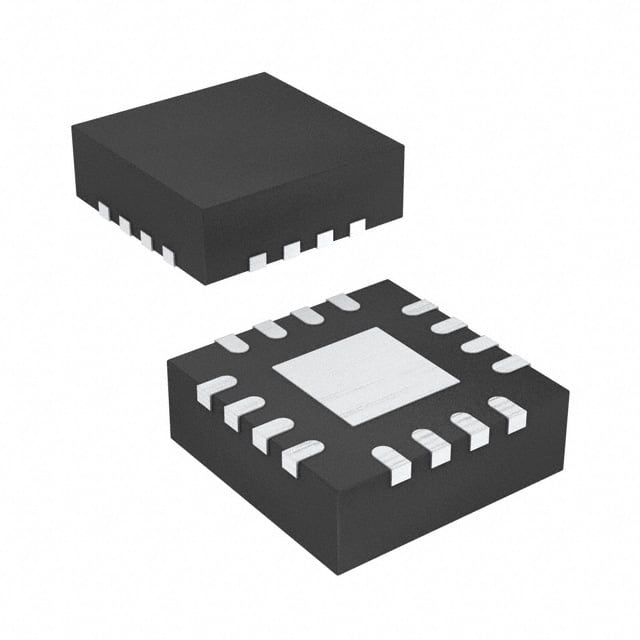
The package of CDCLVD1213RGTT is a small-outline integrated circuit (SOIC) with 16 pins. It is available in tape and reel packaging, with a quantity of 2500 units per reel.
Specifications and Parameters
- Category: Integrated Circuits (ICs)
- Use: Signal transmission and clock distribution
- Characteristics: LVDS, high-speed operation, low power consumption
- Package: SOIC
- Essence: Small-outline integrated circuit
- Packaging/Quantity: Tape and reel, 2500 units per reel
Pin Configuration
The pin configuration of CDCLVD1213RGTT is as follows:
- VCC
- GND
- CLKIN
- CLKOUT0
- CLKOUT1
- CLKOUT2
- CLKOUT3
- CLKOUT4
- CLKOUT5
- CLKOUT6
- CLKOUT7
- CLKOUT8
- CLKOUT9
- CLKOUT10
- CLKOUT11
- NC
Functional Characteristics
CDCLVD1213RGTT provides the following functional characteristics:
- LVDS input and output compatibility
- Clock multiplication and division
- Low jitter and skew
- Wide operating frequency range
- Power-down mode for reduced power consumption
Advantages and Disadvantages
Advantages: - High-speed operation - Low power consumption - LVDS compatibility - Low jitter and skew
Disadvantages: - Limited number of output channels - Requires external clock source
Applicable Range of Products
CDCLVD1213RGTT is commonly used in various electronic devices that require signal transmission and clock distribution, such as:
- Communication equipment
- Data storage systems
- Industrial automation
- Test and measurement instruments
Working Principles
The CDCLVD1213RGTT operates by receiving an input clock signal (CLKIN) and generating multiple output clock signals (CLKOUT0-CLKOUT11) with the desired frequency. It utilizes LVDS technology for high-speed and low-power operation.
Detailed Application Field Plans
CDCLVD1213RGTT can be applied in the following fields:
- Communication Equipment: Used for clock synchronization in network switches and routers.
- Data Storage Systems: Enables precise timing in solid-state drives (SSDs) and hard disk drives (HDDs).
- Industrial Automation: Provides accurate timing for control systems and programmable logic controllers (PLCs).
- Test and Measurement Instruments: Ensures precise timing in oscilloscopes, signal generators, and spectrum analyzers.
Detailed Alternative Models
Some alternative models to CDCLVD1213RGTT include:
- CDCLVD1208RGTT
- CDCLVD1216RGTT
- CDCLVD1220RGTT
- CDCLVD1232RGTT
- CDCLVD1240RGTT
5 Common Technical Questions and Answers
Q: What is the operating voltage range of CDCLVD1213RGTT? A: The operating voltage range is typically between 2.375V and 3.465V.
Q: Can CDCLVD1213RGTT be used in high-speed data transmission applications? A: Yes, CDCLVD1213RGTT is designed for high-speed operation and is suitable for such applications.
Q: Does CDCLVD1213RGTT support power-down mode? A: Yes, CDCLVD1213RGTT features a power-down mode to reduce power consumption when not in use.
Q: What is the maximum operating frequency of CDCLVD1213RGTT? A: The maximum operating frequency is typically 1.5 GHz.
Q: Can CDCLVD1213RGTT be used as a clock multiplier? A: Yes, CDCLVD1213RGTT supports clock multiplication and division functions.
This concludes the encyclopedia entry for CDCLVD1213RGTT.
[Word count: 607]