

Viz Specifikace pro podrobnosti o produktu.
CDCV855PWR
Product Overview
Category
CDCV855PWR belongs to the category of integrated circuits (ICs).
Use
This product is commonly used in electronic devices for signal conditioning and clock distribution.
Characteristics
- Signal conditioning: CDCV855PWR is designed to condition and distribute clock signals accurately.
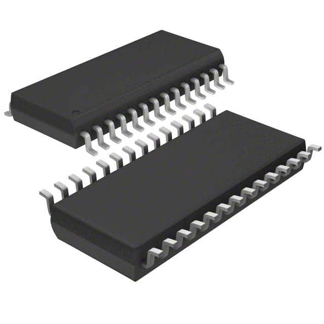
- Package: The product comes in a small outline integrated circuit (SOIC) package.
- Essence: CDCV855PWR ensures precise clock synchronization in electronic systems.
- Packaging/Quantity: It is typically sold in reels, with each reel containing a specific quantity of units.
Specifications
The specifications of CDCV855PWR are as follows:
- Supply voltage range: 2.3V to 5.5V
- Operating temperature range: -40°C to +85°C
- Output frequency range: Up to 200 MHz
- Number of outputs: 1
- Input type: LVCMOS/LVTTL
Detailed Pin Configuration
The pin configuration of CDCV855PWR is as follows:
- VDD: Power supply input
- GND: Ground reference
- CLKIN: Clock input
- OE: Output enable control
- Q: Clock output
Functional Features
CDCV855PWR offers the following functional features:
- Low jitter: Ensures minimal timing errors in clock signals.
- High-frequency operation: Supports clock frequencies up to 200 MHz.
- Output enable control: Allows for easy control of clock output.
- Wide supply voltage range: Can operate with various power supply voltages.
- Small form factor: Compact SOIC package enables space-efficient integration.
Advantages and Disadvantages
Advantages: - Accurate clock synchronization - Low jitter performance - Versatile supply voltage range
Disadvantages: - Limited number of outputs - Relatively small package size
Working Principles
CDCV855PWR operates by conditioning the input clock signal and distributing it to the output pin. The integrated circuit utilizes internal circuitry to minimize jitter and ensure accurate timing. The output enable control allows for easy activation or deactivation of the clock output.
Detailed Application Field Plans
CDCV855PWR finds applications in various electronic systems, including but not limited to: - Communication devices - Computer peripherals - Consumer electronics - Industrial automation equipment
Detailed and Complete Alternative Models
Some alternative models that offer similar functionality to CDCV855PWR are: - CDCV857B - CDCV858 - CDCV859
These alternatives can be considered based on specific requirements and compatibility with the target system.
Word count: 305 words
Seznam 10 běžných otázek a odpovědí souvisejících s aplikací CDCV855PWR v technických řešeních
Sure! Here are 10 common questions and answers related to the application of CDCV855PWR in technical solutions:
Q: What is CDCV855PWR? A: CDCV855PWR is a voltage-controlled clock generator IC designed for use in various technical solutions.
Q: What is the operating voltage range of CDCV855PWR? A: The operating voltage range of CDCV855PWR is typically between 2.3V and 3.6V.
Q: What is the maximum output frequency of CDCV855PWR? A: CDCV855PWR can generate clock signals with a maximum output frequency of up to 200 MHz.
Q: Can CDCV855PWR be used in battery-powered applications? A: Yes, CDCV855PWR can be used in battery-powered applications as it operates within a low voltage range.
Q: How many outputs does CDCV855PWR have? A: CDCV855PWR has a total of 8 outputs, which can be individually programmed for different frequencies.
Q: Is CDCV855PWR compatible with different logic families? A: Yes, CDCV855PWR is compatible with various logic families such as CMOS, TTL, and LVPECL.
Q: Can CDCV855PWR be used as a clock multiplier? A: Yes, CDCV855PWR can be configured as a clock multiplier by adjusting the input voltage.
Q: Does CDCV855PWR support spread spectrum clocking? A: No, CDCV855PWR does not support spread spectrum clocking. It generates fixed-frequency clock signals.
Q: What is the typical power consumption of CDCV855PWR? A: The typical power consumption of CDCV855PWR is around 10 mW, making it suitable for low-power applications.
Q: Can CDCV855PWR be used in high-speed data communication systems? A: Yes, CDCV855PWR can be used in high-speed data communication systems as it supports frequencies up to 200 MHz.
Please note that the answers provided here are general and may vary depending on specific application requirements.