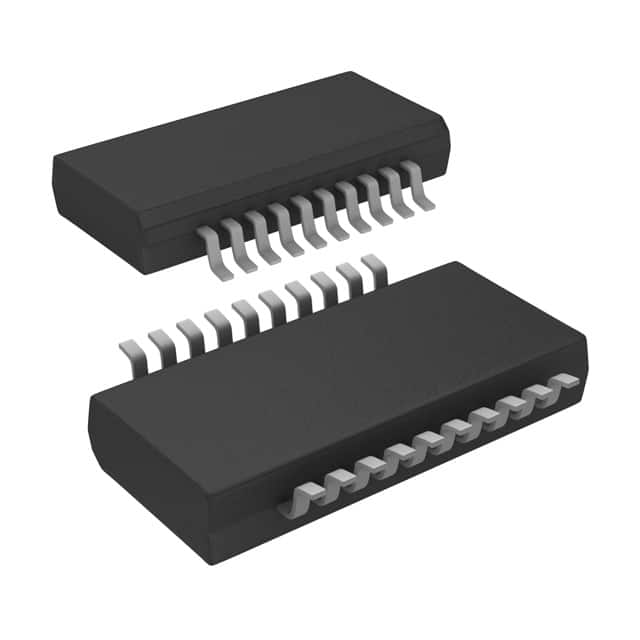
Viz Specifikace pro podrobnosti o produktu.

CY74FCT2541TQCT
Product Overview
Category
CY74FCT2541TQCT belongs to the category of integrated circuits (ICs).
Use
This IC is commonly used in digital electronic systems for signal amplification and buffering.
Characteristics
- High-speed operation
- Low power consumption
- Wide operating voltage range
- Compatibility with various logic families
- Robustness against noise and interference
Package
CY74FCT2541TQCT is available in a small outline integrated circuit (SOIC) package.
Essence
The essence of CY74FCT2541TQCT lies in its ability to amplify and buffer digital signals, ensuring reliable transmission within electronic systems.
Packaging/Quantity
CY74FCT2541TQCT is typically packaged in reels or tubes, with a quantity of 250 or 2,500 units per package.
Specifications
- Supply Voltage: 4.5V to 5.5V
- Input Voltage Range: 0V to VCC
- Output Voltage Range: 0V to VCC
- Operating Temperature Range: -40°C to +85°C
- Logic Family: FCT
Detailed Pin Configuration
CY74FCT2541TQCT consists of 20 pins, each serving a specific function. The pin configuration is as follows:
- OE (Output Enable)
- A1 (Input A1)
- Y1 (Output Y1)
- GND (Ground)
- Y2 (Output Y2)
- A2 (Input A2)
- Y3 (Output Y3)
- A3 (Input A3)
- Y4 (Output Y4)
- A4 (Input A4)
- Y5 (Output Y5)
- A5 (Input A5)
- Y6 (Output Y6)
- A6 (Input A6)
- Y7 (Output Y7)
- A7 (Input A7)
- Y8 (Output Y8)
- VCC (Supply Voltage)
- GND (Ground)
- OE (Output Enable)
Functional Features
- Signal amplification: CY74FCT2541TQCT amplifies weak digital signals, ensuring their integrity and reliability.
- Signal buffering: The IC buffers the amplified signals, preventing degradation during transmission.
- Output enable control: The OE pin allows for enabling or disabling the output signals as needed.
Advantages and Disadvantages
Advantages
- High-speed operation enables efficient signal processing.
- Low power consumption contributes to energy efficiency.
- Wide operating voltage range allows compatibility with various systems.
- Robustness against noise and interference ensures reliable signal transmission.
Disadvantages
- Limited number of input/output channels.
- May require additional components for complex system integration.
Working Principles
CY74FCT2541TQCT operates based on the principles of digital logic circuits. It utilizes transistors and other electronic components to amplify and buffer digital signals. The IC follows specific voltage and timing requirements to ensure accurate signal processing.
Detailed Application Field Plans
CY74FCT2541TQCT finds applications in various fields, including: 1. Communication systems 2. Computer hardware 3. Industrial automation 4. Automotive electronics 5. Consumer electronics
In communication systems, this IC is used for signal conditioning and level shifting. In computer hardware, it aids in data transmission between different components. In industrial automation, it helps in controlling and monitoring processes. In automotive electronics, it plays a role in vehicle control systems. In consumer electronics, it assists in signal routing and processing.
Detailed and Complete Alternative Models
Some alternative models to CY74FCT2541TQCT that serve similar functions include: - SN74FCT2541TQCT - MC74FCT2541TQCT - CD74FCT2541TQCT - 74FCT2541TQCT
These models offer comparable features and can be used as substitutes depending on specific requirements.
Word count: 511 words
Seznam 10 běžných otázek a odpovědí souvisejících s aplikací CY74FCT2541TQCT v technických řešeních
Sure! Here are 10 common questions and answers related to the application of CY74FCT2541TQCT in technical solutions:
1. What is CY74FCT2541TQCT? CY74FCT2541TQCT is a high-speed octal buffer/line driver with 3-state outputs, designed for use as an interface between TTL and CMOS systems.
2. What is the operating voltage range of CY74FCT2541TQCT? The operating voltage range of CY74FCT2541TQCT is from 4.5V to 5.5V.
3. How many inputs and outputs does CY74FCT2541TQCT have? CY74FCT2541TQCT has 8 inputs and 8 outputs.
4. What is the maximum output current of CY74FCT2541TQCT? The maximum output current of CY74FCT2541TQCT is ±24mA.
5. Can CY74FCT2541TQCT be used for level shifting applications? Yes, CY74FCT2541TQCT can be used for level shifting applications as it supports both TTL and CMOS voltage levels.
6. Is CY74FCT2541TQCT suitable for high-speed data transmission? Yes, CY74FCT2541TQCT is designed for high-speed operation and can be used for high-speed data transmission.
7. Does CY74FCT2541TQCT have built-in protection features? Yes, CY74FCT2541TQCT has built-in ESD protection on all inputs and outputs.
8. Can CY74FCT2541TQCT be used in automotive applications? Yes, CY74FCT2541TQCT is qualified for automotive applications and meets the AEC-Q100 standard.
9. What is the typical propagation delay of CY74FCT2541TQCT? The typical propagation delay of CY74FCT2541TQCT is 3.5ns.
10. Can CY74FCT2541TQCT be used in both parallel and serial communication systems? Yes, CY74FCT2541TQCT can be used in both parallel and serial communication systems as a buffer/line driver.
Please note that these answers are based on general information about CY74FCT2541TQCT and may vary depending on specific application requirements. It is always recommended to refer to the datasheet and consult with technical experts for accurate and detailed information.

