

Viz Specifikace pro podrobnosti o produktu.
DAC088S085CISQX
Basic Information Overview
- Category: Digital-to-Analog Converter (DAC)
- Use: Converts digital signals into analog signals
- Characteristics:
- High resolution and accuracy
- Low power consumption
- Small package size
- Wide operating temperature range
- Package: Ceramic quad flat pack (CQFP)
- Essence: Converts binary data to analog voltage or current
- Packaging/Quantity: Individually packaged, quantity per package varies
Specifications
- Resolution: 8 bits
- Number of Channels: 1
- Supply Voltage Range: 2.7V to 5.5V
- Output Type: Voltage or Current
- Output Range: 0V to Vref (Voltage mode), 0mA to Iref (Current mode)
- Operating Temperature Range: -40°C to +125°C
- Interface: Serial Peripheral Interface (SPI)
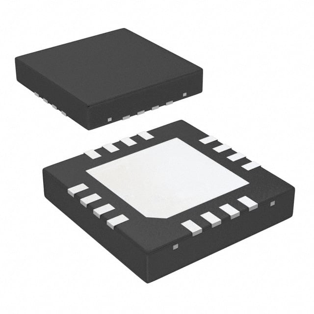
Detailed Pin Configuration
The DAC088S085CISQX has a total of 16 pins. The pin configuration is as follows:
| Pin No. | Pin Name | Description | |---------|----------|-------------| | 1 | VDD | Power supply voltage | | 2 | CS | Chip select input | | 3 | SCLK | Serial clock input | | 4 | DIN | Serial data input | | 5 | GND | Ground | | 6-13 | D0-D7 | Data inputs | | 14 | AGND | Analog ground | | 15 | OUT | Analog output | | 16 | REF | Reference voltage input |
Functional Features
- High-resolution conversion with 8-bit accuracy
- Low power consumption for energy-efficient operation
- Flexible interface allows easy integration with microcontrollers or other digital systems
- Wide operating temperature range enables usage in various environments
- Output can be configured as voltage or current, providing versatility in applications
Advantages and Disadvantages
Advantages
- High resolution and accuracy ensure precise analog signal generation
- Low power consumption reduces energy usage and extends battery life
- Small package size allows for space-efficient designs
- Wide operating temperature range enables usage in extreme conditions
Disadvantages
- Limited to 8-bit resolution, may not be suitable for applications requiring higher precision
- Single-channel output restricts simultaneous conversion of multiple signals
- Requires an external reference voltage for proper operation
Working Principles
The DAC088S085CISQX operates by converting binary data received through the serial interface into corresponding analog voltage or current levels. The digital input is processed internally and converted using a digital-to-analog conversion algorithm. The resulting analog output can be used to control various analog devices or systems.
Detailed Application Field Plans
The DAC088S085CISQX finds applications in various fields, including: 1. Audio Systems: Generating analog audio signals with high fidelity. 2. Industrial Automation: Controlling analog actuators and sensors. 3. Instrumentation: Precise control of analog instruments and equipment. 4. Communication Systems: Generating analog signals for modulation and demodulation processes. 5. Automotive Electronics: Analog control of automotive systems such as motor control and lighting.
Detailed and Complete Alternative Models
- DAC0808LCN: 8-bit Digital-to-Analog Converter with similar features and pin configuration.
- MCP4921-E/P: 12-bit SPI DAC offering higher resolution.
- MAX5216EUB+: 16-bit DAC with extended resolution and enhanced performance.
These alternative models provide options with varying resolutions and additional features to suit different application requirements.
Word count: 457 words
Seznam 10 běžných otázek a odpovědí souvisejících s aplikací DAC088S085CISQX v technických řešeních
Sure! Here are 10 common questions and answers related to the application of DAC088S085CISQX in technical solutions:
Question: What is DAC088S085CISQX?
- Answer: DAC088S085CISQX is a digital-to-analog converter (DAC) integrated circuit that converts digital signals into analog voltage outputs.Question: What is the resolution of DAC088S085CISQX?
- Answer: DAC088S085CISQX has a resolution of 8 bits, meaning it can represent 256 different voltage levels.Question: What is the supply voltage range for DAC088S085CISQX?
- Answer: The supply voltage range for DAC088S085CISQX is typically between 2.7V and 5.5V.Question: Can DAC088S085CISQX be used in both single-ended and differential output configurations?
- Answer: Yes, DAC088S085CISQX supports both single-ended and differential output configurations.Question: What is the maximum output current of DAC088S085CISQX?
- Answer: The maximum output current of DAC088S085CISQX is typically 5 mA.Question: Does DAC088S085CISQX have an internal reference voltage?
- Answer: No, DAC088S085CISQX does not have an internal reference voltage. An external reference voltage must be provided.Question: What is the interface used to communicate with DAC088S085CISQX?
- Answer: DAC088S085CISQX uses a serial interface called SPI (Serial Peripheral Interface) for communication.Question: Can DAC088S085CISQX operate in a power-down mode?
- Answer: Yes, DAC088S085CISQX has a power-down mode that reduces power consumption when not in use.Question: What is the settling time of DAC088S085CISQX?
- Answer: The settling time of DAC088S085CISQX is typically 4.5 µs, which is the time it takes for the output voltage to reach within 1 LSB of its final value.Question: Can multiple DAC088S085CISQX devices be daisy-chained together?
- Answer: Yes, multiple DAC088S085CISQX devices can be daisy-chained together using the SPI interface to control them simultaneously.
Please note that the answers provided here are general and may vary depending on the specific implementation and datasheet of DAC088S085CISQX.