

Viz Specifikace pro podrobnosti o produktu.
DAC7551IDRNT
Product Overview
- Category: Digital-to-Analog Converter (DAC)
- Use: Converts digital signals into analog voltage or current outputs
- Characteristics: High precision, low power consumption, small package size
- Package: Integrated Circuit (IC)
- Essence: Converts binary data to analog signals for various applications
- Packaging/Quantity: Available in tape and reel packaging, quantity varies based on supplier
Specifications
- Resolution: 12 bits
- Number of Channels: 1
- Interface Type: Serial Peripheral Interface (SPI)
- Supply Voltage: 2.7V to 5.5V
- Output Type: Voltage or Current
- Output Range: 0V to Vref (Voltage mode), 4mA to 20mA (Current mode)
- Operating Temperature Range: -40°C to +105°C
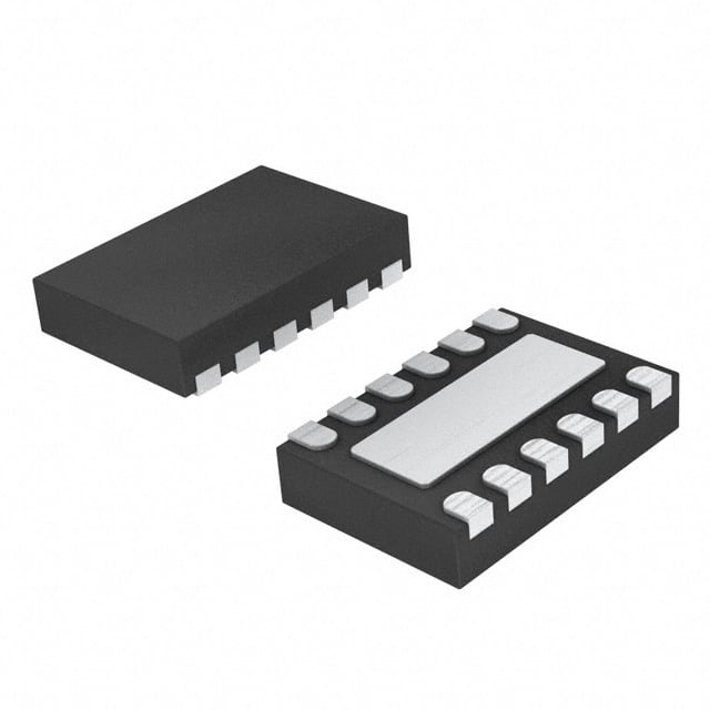
Pin Configuration
The DAC7551IDRNT follows the standard pin configuration for a typical IC package:
```
| | | DAC7551IDRNT | |_______________________________________| | | | 1 2 3 4 5 6 7 8 | |_______________________________________|
Pin 1: VDD (Power supply) Pin 2: GND (Ground) Pin 3: CS (Chip Select) Pin 4: SCLK (Serial Clock) Pin 5: SDI (Serial Data Input) Pin 6: LDAC (Load DAC) Pin 7: REF (Reference Voltage) Pin 8: OUT (Analog Output) ```
Functional Features
- High accuracy and resolution for precise analog output
- Low power consumption for energy-efficient applications
- SPI interface allows easy integration with microcontrollers and other digital systems
- Flexible output options (voltage or current) for versatile usage scenarios
- Internal reference voltage simplifies circuit design
Advantages and Disadvantages
Advantages: - High precision and resolution ensure accurate analog output - Low power consumption extends battery life in portable devices - Small package size saves board space - SPI interface enables easy control and communication
Disadvantages: - Limited to a single channel, not suitable for applications requiring multiple outputs - Operating temperature range may restrict usage in extreme environments
Working Principles
The DAC7551IDRNT operates by converting digital input data into corresponding analog output voltages or currents. It utilizes an internal digital-to-analog conversion technique to accurately translate binary signals into continuous analog signals. The device receives digital data through the SPI interface and converts it into the desired analog output based on the provided reference voltage.
Detailed Application Field Plans
The DAC7551IDRNT finds application in various fields, including:
- Industrial Automation: Control of analog actuators, motor speed control, and process control systems.
- Audio Equipment: Digital audio signal processing, volume control, and equalization.
- Instrumentation: Calibration and testing equipment, sensor signal conditioning, and data acquisition systems.
- Communication Systems: Analog modulation and demodulation, signal generation, and filtering.
- Automotive Electronics: Engine control units, climate control systems, and dashboard displays.
Detailed and Complete Alternative Models
- DAC8551IDGKT: Similar specifications and pin configuration, but with 16-bit resolution.
- MCP4921-E/P: 12-bit DAC with SPI interface, available in DIP package.
- MAX5216EUB+: 16-bit DAC with I2C interface, low power consumption, and small package size.
These alternative models offer similar functionality and can be considered based on specific project requirements.
Word count: 400 words
Seznam 10 běžných otázek a odpovědí souvisejících s aplikací DAC7551IDRNT v technických řešeních
Sure! Here are 10 common questions and answers related to the application of DAC7551IDRNT in technical solutions:
Q1: What is DAC7551IDRNT? A1: DAC7551IDRNT is a digital-to-analog converter (DAC) integrated circuit that converts digital signals into analog voltage or current outputs.
Q2: What is the operating voltage range of DAC7551IDRNT? A2: The operating voltage range of DAC7551IDRNT is typically between 2.7V and 5.5V.
Q3: What is the resolution of DAC7551IDRNT? A3: DAC7551IDRNT has a resolution of 12 bits, which means it can provide 4096 different output levels.
Q4: How does DAC7551IDRNT communicate with a microcontroller or other digital devices? A4: DAC7551IDRNT uses a serial interface such as SPI (Serial Peripheral Interface) or I2C (Inter-Integrated Circuit) to communicate with digital devices.
Q5: Can DAC7551IDRNT generate both voltage and current outputs? A5: Yes, DAC7551IDRNT can be configured to generate either voltage or current outputs based on the application requirements.
Q6: What is the settling time of DAC7551IDRNT? A6: The settling time of DAC7551IDRNT refers to the time it takes for the output voltage or current to stabilize after a change in the input digital value. It typically ranges from a few microseconds to tens of microseconds.
Q7: Is DAC7551IDRNT suitable for precision applications? A7: Yes, DAC7551IDRNT is designed for precision applications and offers low integral non-linearity (INL) and differential non-linearity (DNL) specifications.
Q8: Can DAC7551IDRNT be used in industrial automation systems? A8: Yes, DAC7551IDRNT is commonly used in industrial automation systems for tasks such as controlling motor speed, valve positioning, or generating analog control signals.
Q9: Does DAC7551IDRNT have any built-in reference voltage? A9: No, DAC7551IDRNT requires an external reference voltage to generate accurate analog outputs.
Q10: What are some typical applications of DAC7551IDRNT? A10: Some typical applications of DAC7551IDRNT include audio equipment, instrumentation, process control, data acquisition systems, and programmable logic controllers (PLCs).
Please note that the answers provided here are general and may vary depending on specific datasheet information and application requirements.