

Viz Specifikace pro podrobnosti o produktu.
DS16EV5110ASQ/NOPB
Product Overview
Category
The DS16EV5110ASQ/NOPB belongs to the category of integrated circuits (ICs).
Use
This product is primarily used for signal conditioning and level shifting in high-speed digital communication systems.
Characteristics
- Signal conditioning: The DS16EV5110ASQ/NOPB provides efficient signal conditioning, ensuring reliable data transmission.
- Level shifting: It facilitates seamless interfacing between devices operating at different voltage levels.
- High-speed operation: This IC is designed to handle high-frequency signals, making it suitable for applications requiring fast data transfer.
- Low power consumption: The DS16EV5110ASQ/NOPB is energy-efficient, minimizing power consumption in electronic systems.
- Small form factor: It comes in a compact package, enabling space-saving integration into various electronic designs.
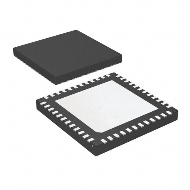
Package and Quantity
The DS16EV5110ASQ/NOPB is available in a small-outline integrated circuit (SOIC) package. Each package contains one unit of the IC.
Specifications
- Supply voltage: 3.3V
- Operating temperature range: -40°C to +85°C
- Data rate: Up to 2.5 Gbps
- Input/output voltage levels: LVDS (Low Voltage Differential Signaling)
- Number of channels: 1
- Input common-mode voltage range: 0V to VCC
- Output swing: 350mV (differential)
Pin Configuration
The DS16EV5110ASQ/NOPB features the following pin configuration:
| Pin Number | Pin Name | Description | |------------|----------|-------------| | 1 | VCC | Power supply voltage input | | 2 | GND | Ground reference | | 3 | INP | Non-inverting differential input | | 4 | INN | Inverting differential input | | 5 | VREF | Reference voltage for input termination | | 6 | OUTP | Non-inverting differential output | | 7 | OUTN | Inverting differential output | | 8 | NC | No connection |
Functional Features
- Signal conditioning: The DS16EV5110ASQ/NOPB amplifies and equalizes the incoming LVDS signals, ensuring optimal signal integrity.
- Level shifting: It converts LVDS signals to a compatible voltage level, allowing seamless interfacing with other devices.
- High-speed operation: This IC supports data rates of up to 2.5 Gbps, enabling fast and reliable data transmission.
- Input termination: The reference voltage (VREF) pin provides input termination for improved signal quality.
- Differential signaling: The non-inverting (OUTP) and inverting (OUTN) differential outputs enable noise-immune data transmission.
Advantages and Disadvantages
Advantages
- Efficient signal conditioning for reliable data transmission
- Seamless interfacing between devices operating at different voltage levels
- High-speed operation for fast data transfer
- Low power consumption for energy-efficient designs
- Compact form factor for space-saving integration
Disadvantages
- Limited to LVDS input/output voltage levels
- Single-channel configuration may not suit applications requiring multiple channels
Working Principles
The DS16EV5110ASQ/NOPB operates based on LVDS technology. It receives LVDS signals through the INP and INN pins, amplifies and equalizes them, and then converts them to a compatible voltage level. The amplified and level-shifted signals are available at the OUTP and OUTN pins for further processing or transmission.
Detailed Application Field Plans
The DS16EV5110ASQ/NOPB finds applications in various fields, including: 1. High-speed data communication systems 2. Telecommunications equipment 3. Industrial automation and control systems 4. Test and measurement instruments 5. Medical imaging devices
Alternative Models
Other alternative models that offer similar functionality to the DS16EV5110ASQ/NOPB include: - SN65LVDS31-Q1 - MAX9126 - DS90LV011A
These alternatives can be considered based on specific design requirements and availability.
In conclusion, the DS16EV5110ASQ/NOPB is a versatile IC used for signal conditioning and level shifting in high-speed digital communication systems. Its efficient operation, low power consumption, and compact form factor make it suitable for various applications. However, its limited voltage compatibility and single-channel configuration should be taken into account during system design.
Seznam 10 běžných otázek a odpovědí souvisejících s aplikací DS16EV5110ASQ/NOPB v technických řešeních
What is the maximum data rate supported by DS16EV5110ASQ/NOPB?
- The maximum data rate supported by DS16EV5110ASQ/NOPB is 2.7 Gbps.What is the operating voltage range of DS16EV5110ASQ/NOPB?
- The operating voltage range of DS16EV5110ASQ/NOPB is from 3.0V to 3.6V.Can DS16EV5110ASQ/NOPB be used in industrial applications?
- Yes, DS16EV5110ASQ/NOPB is suitable for industrial applications.What is the typical power consumption of DS16EV5110ASQ/NOPB?
- The typical power consumption of DS16EV5110ASQ/NOPB is 150mW.Does DS16EV5110ASQ/NOPB support AC-coupled inputs?
- Yes, DS16EV5110ASQ/NOPB supports AC-coupled inputs.Is DS16EV5110ASQ/NOPB compatible with LVDS standards?
- Yes, DS16EV5110ASQ/NOPB is compatible with LVDS standards.What is the temperature range for DS16EV5110ASQ/NOPB?
- The temperature range for DS16EV5110ASQ/NOPB is from -40°C to 85°C.Can DS16EV5110ASQ/NOPB be used in automotive applications?
- Yes, DS16EV5110ASQ/NOPB is suitable for automotive applications.Does DS16EV5110ASQ/NOPB have built-in termination resistors?
- No, DS16EV5110ASQ/NOPB does not have built-in termination resistors.What is the package type of DS16EV5110ASQ/NOPB?
- DS16EV5110ASQ/NOPB comes in a 32-pin WQFN package.