

Viz Specifikace pro podrobnosti o produktu.
P82B96PWG4
Product Overview
- Category: Integrated Circuit
- Use: Bus Extender
- Characteristics: High-speed, bidirectional I2C-bus and SMBus buffer
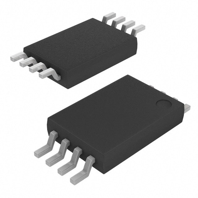
- Package: TSSOP-8
- Essence: Extends the range of I2C-bus and SMBus signals
- Packaging/Quantity: Tape and Reel, 2500 units per reel
Specifications
- Supply Voltage: 2.3V to 5.5V
- Operating Temperature Range: -40°C to +85°C
- I2C-bus/SMBus Compatibility: Compatible with I2C-bus and SMBus standards
- Maximum Frequency: 400 kHz
- Input Capacitance: 10 pF
- Output Capacitance: 20 pF
- Propagation Delay: 1.5 μs (max)
- Low-Level Output Voltage: 0.4V (max)
- High-Level Output Voltage: VCC - 0.4V (min)
Detailed Pin Configuration
The P82B96PWG4 has a total of 8 pins arranged as follows:
- SDA_IN: Input for Serial Data (SDA) signal from the master device.
- SCL_IN: Input for Serial Clock (SCL) signal from the master device.
- GND: Ground reference for the IC.
- VCC: Supply voltage input.
- SDA_OUT: Output for Serial Data (SDA) signal to the slave device.
- SCL_OUT: Output for Serial Clock (SCL) signal to the slave device.
- ENABLE: Enable pin for controlling the bus extender functionality.
- GND: Ground reference for the IC.
Functional Features
- Extends the range of I2C-bus and SMBus signals.
- Provides bidirectional buffering and level shifting for I2C-bus and SMBus signals.
- Supports both standard mode (100 kHz) and fast mode (400 kHz) I2C-bus operation.
- Compatible with I2C-bus and SMBus standards.
- Allows multiple bus extenders to be cascaded for further signal extension.
Advantages
- Enables long-distance communication between I2C-bus devices.
- Provides robust signal buffering and level shifting.
- Supports high-speed data transfer up to 400 kHz.
- Easy to integrate into existing I2C-bus and SMBus systems.
- Low power consumption.
Disadvantages
- Limited to I2C-bus and SMBus applications only.
- Requires additional components for proper operation.
- Not suitable for applications requiring higher data rates.
Working Principles
The P82B96PWG4 is a bus extender designed to extend the range of I2C-bus and SMBus signals. It acts as a buffer and level shifter, allowing communication between devices located far apart. The IC receives the SDA and SCL signals from the master device, buffers them, and then transmits them to the slave device through the SDAOUT and SCLOUT pins. The ENABLE pin controls the bus extender functionality, enabling or disabling the signal transmission.
Detailed Application Field Plans
The P82B96PWG4 finds applications in various fields, including:
- Industrial Automation: Extending I2C-bus communication between sensors, actuators, and control systems.
- Automotive Electronics: Enabling long-distance communication between different modules in a vehicle.
- Consumer Electronics: Facilitating communication between I2C-bus devices in home appliances and entertainment systems.
- Medical Devices: Extending the range of I2C-bus signals in medical equipment for remote monitoring and control.
Detailed and Complete Alternative Models
- PCA9515A: I2C-bus/SMBus level shifting repeater with similar functionality.
- TCA980x: I2C-bus/SMBus repeater and voltage-level translator.
- LTC4316: Hot-swappable I2C-bus buffer with bus capacitance isolation.
These alternative models offer comparable features and can be considered as substitutes for the P82B96PWG4 in different applications.
Word count: 527 words
Seznam 10 běžných otázek a odpovědí souvisejících s aplikací P82B96PWG4 v technických řešeních
Sure! Here are 10 common questions and answers related to the application of P82B96PWG4 in technical solutions:
Q: What is P82B96PWG4? A: P82B96PWG4 is a voltage-level translator and bus buffer IC used for I2C bus applications.
Q: What is the purpose of P82B96PWG4? A: P82B96PWG4 is used to extend the range of I2C bus communication, improve noise immunity, and increase the number of devices that can be connected to the bus.
Q: How does P82B96PWG4 extend the range of I2C bus communication? A: P82B96PWG4 uses a bidirectional bus buffer to convert the logic levels between two I2C buses, allowing them to communicate over longer distances.
Q: Can P82B96PWG4 be used with both standard-mode (100 kHz) and fast-mode (400 kHz) I2C buses? A: Yes, P82B96PWG4 is compatible with both standard-mode and fast-mode I2C buses.
Q: Does P82B96PWG4 require external power supply? A: Yes, P82B96PWG4 requires an external power supply for its operation.
Q: What is the maximum operating voltage for P82B96PWG4? A: The maximum operating voltage for P82B96PWG4 is typically 5.5V.
Q: Can P82B96PWG4 be used in multi-master I2C bus systems? A: Yes, P82B96PWG4 supports multi-master I2C bus systems.
Q: Does P82B96PWG4 support clock stretching? A: Yes, P82B96PWG4 supports clock stretching, which allows devices to hold the clock line low to slow down the communication speed.
Q: Can P82B96PWG4 be used in hot-swapping applications? A: No, P82B96PWG4 is not designed for hot-swapping applications and should not be inserted or removed while the bus is active.
Q: Are there any specific layout considerations for using P82B96PWG4? A: Yes, it is recommended to follow the layout guidelines provided in the datasheet to ensure proper operation and minimize noise interference.
Please note that these answers are general and may vary depending on the specific application and requirements. It is always recommended to refer to the datasheet and consult with the manufacturer for detailed information.