

Viz Specifikace pro podrobnosti o produktu.
SN74AHCT374DGVRE4
Product Overview
- Category: Integrated Circuit (IC)
- Use: Flip-Flop
- Characteristics: High-speed, low-power, 3-state output
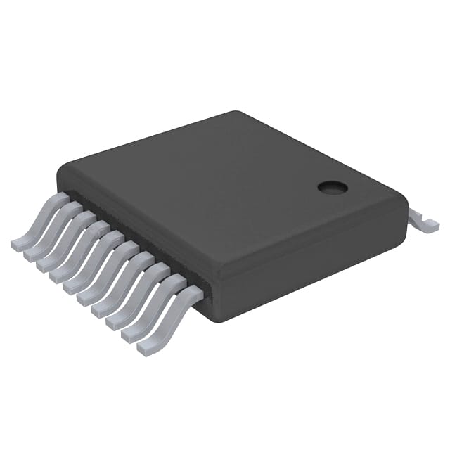
- Package: TSSOP-20
- Essence: D-type flip-flop with 3-state outputs
- Packaging/Quantity: Tape and Reel, 2500 units per reel
Specifications
- Logic Family: AHCT
- Number of Flip-Flops: 8
- Input Voltage Range: 2V to 5.5V
- Output Voltage Range: 0V to VCC
- Propagation Delay Time: 6 ns (typical)
- Operating Temperature Range: -40°C to +85°C
Detailed Pin Configuration
The SN74AHCT374DGVRE4 has a total of 20 pins. The pin configuration is as follows:
- GND (Ground)
- D0 (Data input for flip-flop 0)
- D1 (Data input for flip-flop 1)
- D2 (Data input for flip-flop 2)
- D3 (Data input for flip-flop 3)
- D4 (Data input for flip-flop 4)
- D5 (Data input for flip-flop 5)
- D6 (Data input for flip-flop 6)
- D7 (Data input for flip-flop 7)
- CLK (Clock input)
- OE (Output enable)
- Q0 (Output for flip-flop 0)
- Q1 (Output for flip-flop 1)
- Q2 (Output for flip-flop 2)
- Q3 (Output for flip-flop 3)
- Q4 (Output for flip-flop 4)
- Q5 (Output for flip-flop 5)
- Q6 (Output for flip-flop 6)
- Q7 (Output for flip-flop 7)
- VCC (Power supply)
Functional Features
- D-type flip-flop with 3-state outputs
- High-speed operation
- Low power consumption
- 3-state outputs allow multiple devices to share a common bus
Advantages and Disadvantages
Advantages: - High-speed operation allows for efficient data processing - Low power consumption helps in reducing energy usage - 3-state outputs enable bus sharing, saving on resources
Disadvantages: - Limited number of flip-flops (8 in this case) - Requires external clock signal for proper operation
Working Principles
The SN74AHCT374DGVRE4 is a D-type flip-flop with 3-state outputs. It stores and transfers data based on the clock input. When the clock signal transitions from low to high, the data present at the D inputs is transferred to the corresponding Q outputs. The output enable (OE) pin controls whether the outputs are active or in a high-impedance state.
Detailed Application Field Plans
The SN74AHCT374DGVRE4 can be used in various applications, including:
- Data storage and transfer systems
- Address decoding circuits
- Register banks
- Memory modules
- Bus interface units
Detailed and Complete Alternative Models
Some alternative models that offer similar functionality to the SN74AHCT374DGVRE4 include:
- SN74HC374: High-speed CMOS logic family, 3-state outputs
- CD4013B: Dual D-type flip-flop, 3-state outputs
- MC74ACT374: Advanced CMOS logic family, 3-state outputs
- 74F374: Fast CMOS logic family, 3-state outputs
These alternative models can be considered based on specific requirements and compatibility with existing systems.
Word count: 400 words
Seznam 10 běžných otázek a odpovědí souvisejících s aplikací SN74AHCT374DGVRE4 v technických řešeních
Sure! Here are 10 common questions and answers related to the application of SN74AHCT374DGVRE4 in technical solutions:
Q: What is SN74AHCT374DGVRE4? A: SN74AHCT374DGVRE4 is a type of octal D-type flip-flop integrated circuit (IC) that can be used for data storage and transfer in digital systems.
Q: What is the operating voltage range of SN74AHCT374DGVRE4? A: The operating voltage range of SN74AHCT374DGVRE4 is typically between 4.5V and 5.5V.
Q: How many flip-flops are there in SN74AHCT374DGVRE4? A: SN74AHCT374DGVRE4 contains 8 individual D-type flip-flops, making it an octal flip-flop IC.
Q: What is the maximum clock frequency supported by SN74AHCT374DGVRE4? A: SN74AHCT374DGVRE4 can support clock frequencies up to 100 MHz.
Q: Can SN74AHCT374DGVRE4 be used for both synchronous and asynchronous applications? A: Yes, SN74AHCT374DGVRE4 can be used for both synchronous and asynchronous applications depending on the configuration and connection.
Q: What is the output drive capability of SN74AHCT374DGVRE4? A: SN74AHCT374DGVRE4 has a typical output drive capability of ±24 mA.
Q: Is SN74AHCT374DGVRE4 compatible with other logic families? A: Yes, SN74AHCT374DGVRE4 is compatible with a wide range of logic families, including TTL, CMOS, and LVTTL.
Q: Can SN74AHCT374DGVRE4 be used in high-speed applications? A: Yes, SN74AHCT374DGVRE4 is designed to operate at high speeds and can be used in various high-speed applications.
Q: What is the power supply current consumption of SN74AHCT374DGVRE4? A: The power supply current consumption of SN74AHCT374DGVRE4 depends on the operating conditions but typically ranges from 2 mA to 20 mA.
Q: Are there any special considerations for PCB layout when using SN74AHCT374DGVRE4? A: Yes, it is recommended to follow the manufacturer's guidelines for PCB layout, including proper decoupling capacitors placement and minimizing trace lengths to reduce noise and signal integrity issues.
Please note that these answers are general and may vary depending on specific application requirements and datasheet specifications.