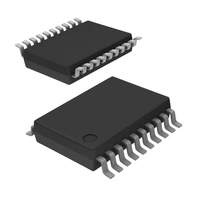
Viz Specifikace pro podrobnosti o produktu.

SN74ALS373ADBR
Product Overview
- Category: Integrated Circuit (IC)
- Use: Octal Transparent D-Type Latches with 3-State Outputs
- Characteristics:
- High-speed operation
- 3-state outputs for bus-oriented applications
- Common latch enable input
- Buffered inputs
- Package: SSOP (Shrink Small Outline Package)
- Essence: Transparent latches with 3-state outputs
- Packaging/Quantity: Tape and Reel, 2500 pieces per reel
Specifications
- Supply Voltage Range: 4.5V to 5.5V
- Input Voltage Range: 0V to VCC
- Output Voltage Range: 0V to VCC
- Operating Temperature Range: -40°C to +85°C
- Input Capacitance: 6pF
- Output Capacitance: 12pF
- Propagation Delay Time: 7ns
- Maximum Quiescent Supply Current: 80μA
Detailed Pin Configuration
The SN74ALS373ADBR has a 20-pin SSOP package with the following pin configuration:
- D0
- D1
- D2
- D3
- D4
- D5
- D6
- D7
- GND (Ground)
- LE (Latch Enable)
- OE (Output Enable)
- Q0
- Q1
- Q2
- Q3
- Q4
- Q5
- Q6
- Q7
- VCC (Supply Voltage)
Functional Features
- Octal transparent latches with 3-state outputs
- Latch enable input controls the state of the outputs
- Output enable input allows the outputs to be disabled
- Buffered inputs ensure signal integrity
- High-speed operation for efficient data transfer
Advantages and Disadvantages
Advantages: - High-speed operation allows for quick data processing - 3-state outputs enable bus-oriented applications - Buffered inputs enhance signal quality - Common latch enable input simplifies control logic
Disadvantages: - Limited supply voltage range (4.5V to 5.5V) - Relatively high input and output capacitance - Propagation delay time of 7ns may not be suitable for ultra-fast applications
Working Principles
The SN74ALS373ADBR is an octal transparent latch with 3-state outputs. It operates by latching the input data when the latch enable (LE) input is high. The state of the outputs can be controlled by the output enable (OE) input. When OE is low, the outputs are enabled and reflect the latched input data. When OE is high, the outputs are in a high-impedance state.
The buffered inputs ensure that the input signals are properly amplified and can drive the internal circuitry. This helps maintain signal integrity and reduces the risk of data corruption.
Detailed Application Field Plans
The SN74ALS373ADBR is commonly used in various applications, including:
- Data storage systems
- Address decoding circuits
- Bus interface units
- Memory modules
- Microprocessor-based systems
Its ability to handle multiple data inputs and provide 3-state outputs makes it suitable for applications where data transfer and control are critical.
Detailed and Complete Alternative Models
- SN74ALS374ADW - Octal D-Type Flip-Flop with 3-State Outputs
- SN74ALS573BDWR - Octal D-Type Transparent Latches with 3-State Outputs
- SN74ALS574BDWR - Octal D-Type Flip-Flop with 3-State Outputs
These alternative models offer similar functionality and can be used as substitutes for the SN74ALS373ADBR in various applications.
Word count: 410 words
Seznam 10 běžných otázek a odpovědí souvisejících s aplikací SN74ALS373ADBR v technických řešeních
Sure! Here are 10 common questions and answers related to the application of SN74ALS373ADBR in technical solutions:
Q: What is SN74ALS373ADBR? A: SN74ALS373ADBR is a type of octal transparent latch with 3-state outputs, commonly used in digital systems.
Q: What is the purpose of SN74ALS373ADBR? A: It is used to store and control the flow of data in digital circuits, allowing for efficient data transfer between different components.
Q: How many bits can SN74ALS373ADBR handle? A: SN74ALS373ADBR can handle 8 bits of data, as it is an octal latch.
Q: What is the voltage range supported by SN74ALS373ADBR? A: SN74ALS373ADBR supports a voltage range of 2V to 6V.
Q: Can SN74ALS373ADBR be used in both synchronous and asynchronous applications? A: Yes, SN74ALS373ADBR can be used in both synchronous and asynchronous applications, depending on the requirements of the system.
Q: What is the maximum operating frequency of SN74ALS373ADBR? A: The maximum operating frequency of SN74ALS373ADBR is typically around 100 MHz.
Q: Does SN74ALS373ADBR have any built-in protection features? A: Yes, SN74ALS373ADBR has built-in diode clamps to protect against electrostatic discharge (ESD) events.
Q: Can SN74ALS373ADBR drive LEDs directly? A: No, SN74ALS373ADBR is not designed to drive LEDs directly. It is primarily used for data storage and transfer.
Q: What is the power supply voltage required for SN74ALS373ADBR? A: SN74ALS373ADBR requires a power supply voltage of 5V.
Q: Can SN74ALS373ADBR be cascaded to handle more than 8 bits of data? A: Yes, multiple SN74ALS373ADBR latches can be cascaded together to handle larger data widths in digital systems.
Please note that these answers are general and may vary depending on specific application requirements and datasheet specifications.

