

Viz Specifikace pro podrobnosti o produktu.
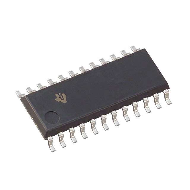
SN74ALS870NSR
Product Overview
- Category: Integrated Circuit (IC)
- Use: Logic Function
- Characteristics: High-Speed, Low-Power, TTL-Compatible
- Package: 20-pin Small Outline Integrated Circuit (SOIC)
- Essence: The SN74ALS870NSR is a high-speed octal transparent latch with 3-state outputs. It is designed for use in various digital logic applications.
- Packaging/Quantity: Available in reels of 2500 units
Specifications
- Supply Voltage: 4.5V to 5.5V
- Input Voltage: 0V to VCC
- Output Voltage: 0V to VCC
- Operating Temperature: -40°C to +85°C
- Propagation Delay: 6ns (typical)
- Output Current: ±24mA
Pin Configuration
The SN74ALS870NSR has a 20-pin configuration as follows:
- GND (Ground)
- D0 (Data Input 0)
- D1 (Data Input 1)
- D2 (Data Input 2)
- D3 (Data Input 3)
- D4 (Data Input 4)
- D5 (Data Input 5)
- D6 (Data Input 6)
- D7 (Data Input 7)
- LE (Latch Enable)
- OE (Output Enable)
- Q0 (Output 0)
- Q1 (Output 1)
- Q2 (Output 2)
- Q3 (Output 3)
- Q4 (Output 4)
- Q5 (Output 5)
- Q6 (Output 6)
- Q7 (Output 7)
- VCC (Supply Voltage)
Functional Features
- Octal transparent latch with 3-state outputs
- Latch enable and output enable control signals
- High-speed operation
- TTL-compatible inputs and outputs
- Low-power consumption
Advantages and Disadvantages
Advantages: - High-speed operation allows for efficient data handling - Low-power consumption helps in reducing overall power requirements - TTL compatibility ensures easy integration with existing logic circuits
Disadvantages: - Limited number of outputs may restrict certain applications requiring more outputs - Propagation delay of 6ns may not be suitable for ultra-high-speed applications
Working Principles
The SN74ALS870NSR operates as an octal transparent latch. When the latch enable (LE) signal is high, the data inputs (D0-D7) are transferred to the outputs (Q0-Q7). The output enable (OE) signal controls whether the outputs are active or in a high-impedance state.
Detailed Application Field Plans
The SN74ALS870NSR can be used in various digital logic applications, including but not limited to: - Data storage and transfer systems - Address decoding circuits - Bus interface units - Register banks - Multiplexers and demultiplexers
Detailed and Complete Alternative Models
Some alternative models that can be considered as alternatives to the SN74ALS870NSR are: - SN74LS373N - SN74HC573AN - CD74ACT273M
These models offer similar functionality and characteristics, providing options for different design requirements.
In conclusion, the SN74ALS870NSR is a high-speed octal transparent latch with 3-state outputs. It offers advantages such as high-speed operation, low-power consumption, and TTL compatibility. However, it has limitations in terms of the number of outputs and propagation delay. It finds applications in various digital logic systems and has alternative models available for different design needs.
Seznam 10 běžných otázek a odpovědí souvisejících s aplikací SN74ALS870NSR v technických řešeních
Sure! Here are 10 common questions and answers related to the application of SN74ALS870NSR:
Q: What is SN74ALS870NSR? A: SN74ALS870NSR is a specific model of integrated circuit (IC) manufactured by Texas Instruments. It is a 10-bit transparent latch with 3-state outputs.
Q: What are the typical applications of SN74ALS870NSR? A: SN74ALS870NSR can be used in various technical solutions, such as data storage, address decoding, bus interfacing, and general-purpose digital logic circuits.
Q: What is the operating voltage range for SN74ALS870NSR? A: SN74ALS870NSR operates within a voltage range of 4.5V to 5.5V.
Q: How many inputs and outputs does SN74ALS870NSR have? A: SN74ALS870NSR has 10 inputs and 10 outputs.
Q: What is the maximum clock frequency supported by SN74ALS870NSR? A: SN74ALS870NSR can operate at a maximum clock frequency of 25 MHz.
Q: Does SN74ALS870NSR support 3-state outputs? A: Yes, SN74ALS870NSR has 3-state outputs, which means it can effectively disconnect its outputs from the bus when not in use.
Q: Can SN74ALS870NSR be cascaded to increase the number of bits? A: Yes, multiple SN74ALS870NSR ICs can be cascaded together to increase the number of bits in the latch.
Q: Is SN74ALS870NSR compatible with TTL logic levels? A: Yes, SN74ALS870NSR is compatible with TTL logic levels, making it suitable for interfacing with other TTL devices.
Q: What is the power consumption of SN74ALS870NSR? A: The power consumption of SN74ALS870NSR depends on various factors such as clock frequency and load conditions. Please refer to the datasheet for detailed information.
Q: Are there any specific precautions to consider when using SN74ALS870NSR? A: It is important to follow the recommended operating conditions and guidelines provided in the datasheet. Proper decoupling capacitors and signal integrity measures should be implemented for optimal performance.
Please note that these answers are general and may vary depending on the specific application and requirements. Always refer to the official documentation and datasheet for accurate and up-to-date information.