

Viz Specifikace pro podrobnosti o produktu.
SN74ALS874BNSRE4
Product Overview
- Category: Integrated Circuit (IC)
- Use: Logic Function
- Characteristics: High-speed, Low-power, TTL-Compatible
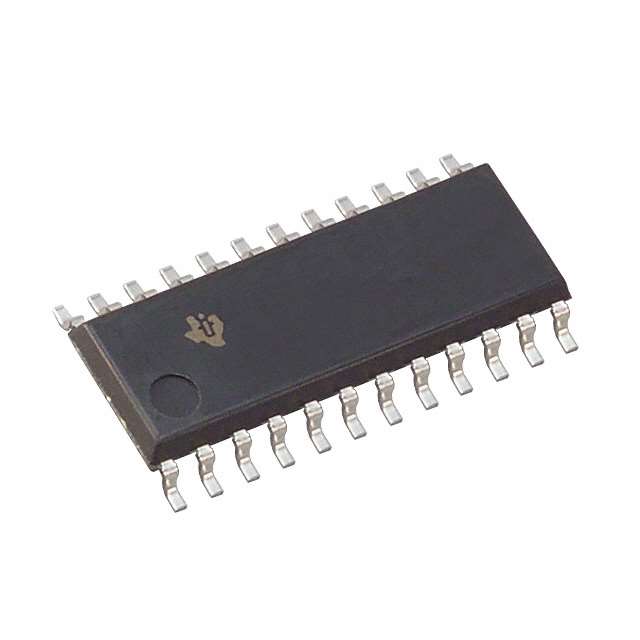
- Package: SOIC (Small Outline Integrated Circuit)
- Essence: 8-Bit D-Type Flip-Flop with 3-State Outputs
- Packaging/Quantity: Tape and Reel, 2500 units per reel
Specifications
- Supply Voltage Range: 4.5V to 5.5V
- Input Voltage Range: 0V to VCC
- Output Voltage Range: 0V to VCC
- Operating Temperature Range: -40°C to +85°C
- Propagation Delay Time: 7ns (typical)
- Output Current: ±24mA
- Input Capacitance: 3pF
- Output Capacitance: 15pF
Detailed Pin Configuration
The SN74ALS874BNSRE4 has a total of 20 pins. The pin configuration is as follows:
- CLR (Clear) - Active LOW clear input
- D0-D7 (Data Inputs) - Eight data inputs
- CP (Clock Pulse) - Clock pulse input
- OE (Output Enable) - Active LOW output enable input
- Q0-Q7 (Flip-Flop Outputs) - Eight flip-flop outputs
- GND (Ground) - Ground reference
- Q7' (Complementary Output) - Complementary output of Q7
- VCC (Supply Voltage) - Positive supply voltage
Functional Features
- 8-bit D-type flip-flop with 3-state outputs
- Synchronous operation with common clock
- Asynchronous active LOW clear
- 3-state outputs for bus-oriented applications
- TTL-compatible inputs and outputs
- High-speed operation with low power consumption
Advantages and Disadvantages
Advantages: - High-speed operation allows for efficient data processing - Low-power consumption helps in reducing energy usage - TTL-compatible inputs and outputs ensure compatibility with other logic devices - 3-state outputs enable bus-oriented applications
Disadvantages: - Limited operating temperature range (-40°C to +85°C) - Input and output voltage range limited to the supply voltage range (0V to VCC)
Working Principles
The SN74ALS874BNSRE4 is an 8-bit D-type flip-flop with 3-state outputs. It operates synchronously with a common clock pulse input (CP). The data inputs (D0-D7) are latched into the flip-flops on the rising edge of the clock pulse. The clear input (CLR) is asynchronous and active LOW, allowing for the clearing of all flip-flops when activated. The output enable input (OE) is active LOW and controls the 3-state outputs (Q0-Q7), enabling or disabling their functionality.
Detailed Application Field Plans
The SN74ALS874BNSRE4 is commonly used in various digital systems and applications, including:
- Microprocessors and microcontrollers
- Data storage systems
- Communication systems
- Industrial automation
- Automotive electronics
- Consumer electronics
Its high-speed operation, low-power consumption, and compatibility with TTL logic make it suitable for these applications.
Detailed and Complete Alternative Models
- SN74ALS876BNSRE4: 16-Bit D-Type Flip-Flop with 3-State Outputs
- SN74ALS872BNSRE4: 4-Bit D-Type Flip-Flop with 3-State Outputs
- SN74ALS878BNSRE4: 8-Bit Transparent Latch with 3-State Outputs
- SN74ALS870BNSRE4: Octal D-Type Transparent Latch with 3-State Outputs
These alternative models offer similar functionality and characteristics, providing options for different design requirements.
In conclusion, the SN74ALS874BNSRE4 is an 8-bit D-type flip-flop with 3-state outputs. It offers high-speed operation, low-power consumption, and compatibility with TTL logic. With its various applications and alternative models available, it serves as a versatile component in digital systems.
Seznam 10 běžných otázek a odpovědí souvisejících s aplikací SN74ALS874BNSRE4 v technických řešeních
Sure! Here are 10 common questions and answers related to the application of SN74ALS874BNSRE4 in technical solutions:
Q: What is SN74ALS874BNSRE4? A: SN74ALS874BNSRE4 is a specific model of integrated circuit (IC) that belongs to the ALS family of logic devices.
Q: What is the function of SN74ALS874BNSRE4? A: SN74ALS874BNSRE4 is an octal D-type transparent latch with 3-state outputs. It can store data and control the flow of information in a digital system.
Q: What is the operating voltage range for SN74ALS874BNSRE4? A: The operating voltage range for SN74ALS874BNSRE4 is typically between 4.5V and 5.5V.
Q: How many latches are there in SN74ALS874BNSRE4? A: SN74ALS874BNSRE4 has 8 individual latches, making it an octal latch.
Q: What is the maximum clock frequency supported by SN74ALS874BNSRE4? A: SN74ALS874BNSRE4 can operate at a maximum clock frequency of 25 MHz.
Q: Can SN74ALS874BNSRE4 be used in both parallel and serial data transfer applications? A: Yes, SN74ALS874BNSRE4 can be used in both parallel and serial data transfer applications, depending on the configuration and connection.
Q: What is the output drive capability of SN74ALS874BNSRE4? A: SN74ALS874BNSRE4 has a typical output drive capability of ±24 mA.
Q: Does SN74ALS874BNSRE4 have any built-in protection features? A: Yes, SN74ALS874BNSRE4 has built-in diode clamps to protect against electrostatic discharge (ESD) and other voltage spikes.
Q: Can SN74ALS874BNSRE4 be used in both commercial and industrial applications? A: Yes, SN74ALS874BNSRE4 is designed to operate reliably in both commercial and industrial temperature ranges.
Q: What are some typical applications of SN74ALS874BNSRE4? A: SN74ALS874BNSRE4 can be used in various applications such as data storage, address decoding, bus interfacing, and general-purpose digital logic circuits.
Please note that the answers provided here are general and may vary depending on the specific requirements and datasheet of SN74ALS874BNSRE4.