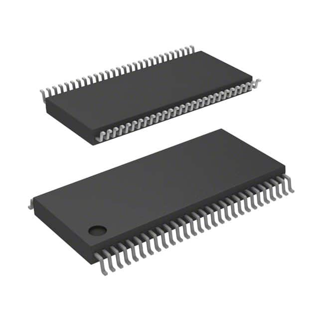
Viz Specifikace pro podrobnosti o produktu.

SN74ALVCH16903DGGR
Product Overview
- Category: Integrated Circuit (IC)
- Use: Logic Level Translator
- Characteristics: High-speed, low-power, voltage-level shifting
- Package: TSSOP-56
- Essence: Logic level translation between different voltage domains
- Packaging/Quantity: Tape and Reel, 2500 units per reel
Specifications
- Supply Voltage Range: 1.2V to 3.6V
- Input Voltage Range: 0V to VCC
- Output Voltage Range: 0V to VCC
- Operating Temperature Range: -40°C to +85°C
- Propagation Delay: 2.5ns (typical)
- Maximum Frequency: 500MHz
Detailed Pin Configuration
The SN74ALVCH16903DGGR has a total of 56 pins. The pin configuration is as follows:
- A1
- Y1
- B1
- GND
- A2
- Y2
- B2
- VCC
- A3
- Y3
- B3
- GND
- A4
- Y4
- B4
- VCC
- A5
- Y5
- B5
- GND
- A6
- Y6
- B6
- VCC
- A7
- Y7
- B7
- GND
- A8
- Y8
- B8
- VCC
- A9
- Y9
- B9
- GND
- A10
- Y10
- B10
- VCC
- A11
- Y11
- B11
- GND
- A12
- Y12
- B12
- VCC
- A13
- Y13
- B13
- GND
- A14
- Y14
- B14
- VCC
Functional Features
- Logic level translation between different voltage domains
- Bidirectional voltage-level shifting
- High-speed operation with minimal propagation delay
- Low power consumption
- Supports a wide supply voltage range
Advantages and Disadvantages
Advantages: - Enables communication between devices operating at different voltage levels - High-speed operation allows for efficient data transfer - Low power consumption helps conserve energy - Wide supply voltage range provides flexibility in various applications
Disadvantages: - Limited to 14-bit translation, may not be suitable for larger data buses - Requires careful consideration of input and output voltage levels to ensure proper functionality
Working Principles
The SN74ALVCH16903DGGR is designed to translate logic levels between different voltage domains. It utilizes a combination of MOSFETs and CMOS technology to achieve bidirectional voltage-level shifting. The device operates by detecting the input voltage level and translating it to the corresponding output voltage level based on the specified voltage thresholds. This enables seamless communication between devices operating at different voltage levels.
Detailed Application Field Plans
The SN74ALVCH16903DGGR can be used in various applications where logic level translation is required. Some potential application fields include:
- Microcontroller interfacing: Facilitating communication between microcontrollers operating at different voltage levels.
- Sensor networks: Enabling connectivity between sensors and control units with varying voltage requirements.
- Industrial automation: Integrating different subsystems with distinct voltage domains in industrial control systems.
- Consumer electronics: Supporting voltage-level translation in devices such as smartphones, tablets, and gaming consoles.
Detailed and Complete Alternative Models
- SN74LVC1T45DBVR: Single-bit voltage level translator with a smaller package size (SOT-23).
- TXB0108PWR: 8-bit bidirectional voltage-level translator with enhanced ESD protection.
- PCA9306DCUR: Dual bidirectional I2C-bus and SMBus voltage-level translator with automatic direction sensing.
These alternative models offer similar functionality to the SN74ALVCH16903DGGR and can be considered based on specific application requirements.
Word count: 511 words
Seznam 10 běžných otázek a odpovědí souvisejících s aplikací SN74ALVCH16903DGGR v technických řešeních
Sure! Here are 10 common questions and answers related to the application of SN74ALVCH16903DGGR:
Q: What is SN74ALVCH16903DGGR? A: SN74ALVCH16903DGGR is a 12-bit universal bus driver with 3-state outputs, designed for low-voltage (1.65V to 3.6V) applications.
Q: What are the typical applications of SN74ALVCH16903DGGR? A: SN74ALVCH16903DGGR is commonly used in various technical solutions such as data communication systems, networking equipment, industrial automation, and embedded systems.
Q: What is the maximum operating frequency of SN74ALVCH16903DGGR? A: The maximum operating frequency of SN74ALVCH16903DGGR is typically around 400 MHz.
Q: How many output channels does SN74ALVCH16903DGGR have? A: SN74ALVCH16903DGGR has 12 output channels, each capable of driving up to 24 mA.
Q: Can SN74ALVCH16903DGGR be used with different voltage levels? A: Yes, SN74ALVCH16903DGGR supports voltage translation between different voltage levels, making it suitable for interfacing between different logic families.
Q: Does SN74ALVCH16903DGGR have built-in ESD protection? A: Yes, SN74ALVCH16903DGGR has built-in ESD protection, which helps protect the device from electrostatic discharge events.
Q: What is the power supply voltage range for SN74ALVCH16903DGGR? A: SN74ALVCH16903DGGR operates with a power supply voltage range of 1.65V to 3.6V.
Q: Can SN74ALVCH16903DGGR be used in high-speed data transmission applications? A: Yes, SN74ALVCH16903DGGR is designed to support high-speed data transmission and can be used in applications requiring fast signal switching.
Q: Does SN74ALVCH16903DGGR have any special features for reducing power consumption? A: Yes, SN74ALVCH16903DGGR incorporates advanced power-saving features such as partial power-down mode and bus-hold functionality to minimize power consumption.
Q: Is SN74ALVCH16903DGGR available in different package options? A: Yes, SN74ALVCH16903DGGR is available in various package options, including TSSOP, VQFN, and SOIC, providing flexibility for different PCB layouts and assembly processes.
Please note that the answers provided here are general and may vary depending on the specific datasheet and application requirements.

