

Viz Specifikace pro podrobnosti o produktu.
SN74ALVCH16903DGVR
Basic Information Overview
- Category: Integrated Circuit (IC)
- Use: Logic Level Translator
- Characteristics:
- Wide voltage range translation (1.2V to 3.6V)
- High-speed operation (up to 400 Mbps)
- Low power consumption
- Schmitt-trigger inputs for noise immunity
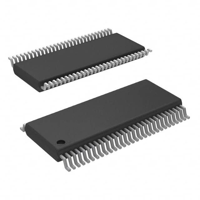
- Package: VSSOP (Very Small Outline Package)
- Essence: Logic level translation between different voltage domains
- Packaging/Quantity: Tape and Reel, 2500 units per reel
Specifications
- Supply Voltage Range: 1.2V to 3.6V
- Input Voltage Range (A Port): 0V to VCCA + 0.5V
- Input Voltage Range (B Port): 0V to VCCB + 0.5V
- Output Voltage Range (A Port): 0V to VCCA + 0.5V
- Output Voltage Range (B Port): 0V to VCCB + 0.5V
- Maximum Propagation Delay: 4.7 ns
- Operating Temperature Range: -40°C to 85°C
Detailed Pin Configuration
The SN74ALVCH16903DGVR has a total of 56 pins, arranged as follows:
___________
      |           |
   1  |         56 |  VCCA
   2  |         55 |  GND
   3  |         54 |  A1
   4  |         53 |  B1
   .  |         .  |  .
   .  |         .  |  .
   .  |         .  |  .
   27 |         30 |  Y28
   28 |         29 |  GND
      |___________|
Functional Features
- Logic level translation between two voltage domains (A and B ports)
- Bidirectional data flow
- Automatic direction control based on the voltage levels of VCCA and VCCB
Advantages
- Wide voltage range translation allows compatibility with various systems
- High-speed operation enables fast data transfer
- Low power consumption helps in reducing overall system power requirements
- Schmitt-trigger inputs provide noise immunity, ensuring reliable operation
Disadvantages
- Limited to logic level translation and does not perform other functions
- Not suitable for applications requiring voltage translation beyond the specified range
Working Principles
The SN74ALVCH16903DGVR is a bidirectional logic level translator that operates by monitoring the voltage levels of the VCCA and VCCB pins. When the voltage at VCCA is higher than VCCB, the A port is considered the high-voltage side, and the B port is considered the low-voltage side. Conversely, when the voltage at VCCB is higher than VCCA, the A port becomes the low-voltage side, and the B port becomes the high-voltage side. The device automatically controls the direction of data flow based on this voltage comparison.
Detailed Application Field Plans
The SN74ALVCH16903DGVR is commonly used in various applications where logic level translation is required between different voltage domains. Some specific application fields include: - Microcontrollers interfacing with sensors or peripheral devices operating at different voltage levels - Communication systems involving multiple voltage domains, such as UART, I2C, SPI interfaces - Battery-powered devices where low power consumption is crucial
Detailed and Complete Alternative Models
- SN74LVC1T45DBVR
- SN74AVC4T245RGYR
- SN74LV1T34DBVR
- SN74LVC2T45DCTR
- SN74AVC4T245PWRE4
These alternative models offer similar logic level translation capabilities and can be considered as substitutes for the SN74ALVCH16903DGVR in various applications.
Word count: 430 words
Seznam 10 běžných otázek a odpovědí souvisejících s aplikací SN74ALVCH16903DGVR v technických řešeních
Sure! Here are 10 common questions and answers related to the application of SN74ALVCH16903DGVR:
1. What is SN74ALVCH16903DGVR? - SN74ALVCH16903DGVR is a 12-bit universal bus driver with 3-state outputs. It is commonly used in digital systems for driving and receiving signals.
2. What is the operating voltage range of SN74ALVCH16903DGVR? - The operating voltage range of SN74ALVCH16903DGVR is from 1.65V to 3.6V.
3. How many output pins does SN74ALVCH16903DGVR have? - SN74ALVCH16903DGVR has 12 output pins, each capable of driving up to 32mA.
4. Can SN74ALVCH16903DGVR be used as a level shifter? - Yes, SN74ALVCH16903DGVR can be used as a level shifter as it supports bidirectional voltage translation between different voltage domains.
5. What is the maximum data rate supported by SN74ALVCH16903DGVR? - SN74ALVCH16903DGVR supports a maximum data rate of 400Mbps.
6. Is SN74ALVCH16903DGVR compatible with other logic families? - Yes, SN74ALVCH16903DGVR is compatible with various logic families such as TTL, CMOS, and LVCMOS.
7. Can SN74ALVCH16903DGVR be used in high-speed applications? - Yes, SN74ALVCH16903DGVR is designed for high-speed operation and can be used in applications that require fast signal propagation.
8. Does SN74ALVCH16903DGVR have built-in ESD protection? - Yes, SN74ALVCH16903DGVR has built-in ESD protection on all inputs and outputs, making it more robust against electrostatic discharge.
9. What is the power supply current of SN74ALVCH16903DGVR? - The power supply current of SN74ALVCH16903DGVR depends on the operating conditions but typically ranges from 2mA to 10mA.
10. Can SN74ALVCH16903DGVR be used in automotive applications? - Yes, SN74ALVCH16903DGVR is qualified for automotive applications and meets the AEC-Q100 standard.
Please note that these answers are general and may vary depending on specific application requirements. It is always recommended to refer to the datasheet and consult with the manufacturer for detailed information.