

Viz Specifikace pro podrobnosti o produktu.
SN74AUC2G79YZPR
Product Overview
- Category: Integrated Circuit (IC)
- Use: Logic Gate
- Characteristics: Dual Positive-Edge-Triggered D-Type Flip-Flop
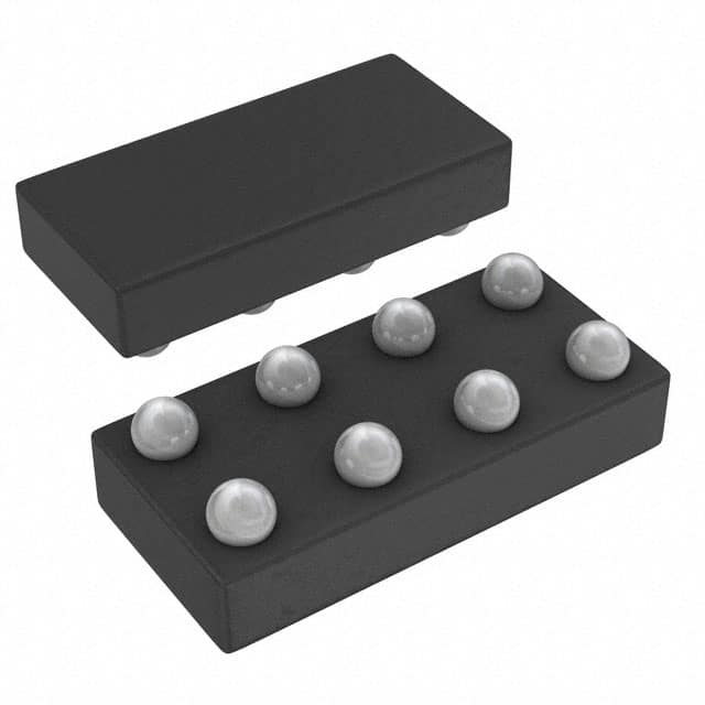
- Package: 8-Bump micro SMD
- Essence: High-speed, low-power consumption flip-flop
- Packaging/Quantity: Tape and Reel, 3000 units per reel
Specifications
The SN74AUC2G79YZPR is a dual positive-edge-triggered D-type flip-flop integrated circuit. It operates at high speed while consuming low power. The flip-flop is designed to store and transfer data in digital systems. It features two independent flip-flops with common clock and reset inputs.
Detailed Pin Configuration
The SN74AUC2G79YZPR has a total of 8 pins, which are assigned as follows:
- Pin 1: Data Input A
- Pin 2: Clock Input
- Pin 3: Reset Input
- Pin 4: Data Output A
- Pin 5: Data Input B
- Pin 6: GND (Ground)
- Pin 7: VCC (Power Supply)
- Pin 8: Data Output B
Functional Features
- Positive-edge-triggered operation
- Independent clock and reset inputs for each flip-flop
- Low power consumption
- High-speed operation
- Wide operating voltage range
Advantages and Disadvantages
Advantages: - High-speed operation allows for efficient data transfer - Low power consumption helps in reducing overall system power requirements - Independent clock and reset inputs provide flexibility in controlling the flip-flop's behavior
Disadvantages: - Limited number of flip-flops in a single package - Small form factor may require additional care during handling and soldering
Working Principles
The SN74AUC2G79YZPR operates based on positive-edge-triggered D-type flip-flop principles. When the clock input transitions from low to high (positive edge), the data at the input is transferred to the output. The reset input can be used to clear the flip-flop and set the output to a known state.
Detailed Application Field Plans
The SN74AUC2G79YZPR is commonly used in various digital systems where the storage and transfer of data is required. Some specific application fields include:
- Communication Systems: Used for data buffering and synchronization.
- Microcontrollers: Employed for storing intermediate results and controlling sequential operations.
- Data Processing Units: Utilized for temporary data storage and synchronization.
Detailed and Complete Alternative Models
- SN74AUC2G79DCUR: Similar dual positive-edge-triggered D-type flip-flop with different package type (SOT-23).
- SN74AUC2G79DCTR: Dual positive-edge-triggered D-type flip-flop with extended temperature range (-40°C to 125°C).
- SN74AUC2G79DBVR: Single positive-edge-triggered D-type flip-flop with smaller package size (SOT-23).
These alternative models provide similar functionality but may differ in package type, temperature range, or number of flip-flops per package.
Word count: 346 words
Seznam 10 běžných otázek a odpovědí souvisejících s aplikací SN74AUC2G79YZPR v technických řešeních
Sure! Here are 10 common questions and answers related to the application of SN74AUC2G79YZPR in technical solutions:
Q: What is SN74AUC2G79YZPR? A: SN74AUC2G79YZPR is a dual positive-edge-triggered D-type flip-flop with clear, designed for 1.65-V to 3.6-V VCC operation.
Q: What are the key features of SN74AUC2G79YZPR? A: The key features include low power consumption, wide operating voltage range, high-speed operation, and small package size.
Q: What is the maximum operating frequency of SN74AUC2G79YZPR? A: The maximum operating frequency of SN74AUC2G79YZPR is typically around 500 MHz.
Q: What is the power supply voltage range for SN74AUC2G79YZPR? A: SN74AUC2G79YZPR operates within a power supply voltage range of 1.65V to 3.6V.
Q: Can SN74AUC2G79YZPR be used in battery-powered applications? A: Yes, SN74AUC2G79YZPR is suitable for battery-powered applications due to its low power consumption.
Q: What is the typical propagation delay of SN74AUC2G79YZPR? A: The typical propagation delay of SN74AUC2G79YZPR is around 2.8 ns.
Q: Does SN74AUC2G79YZPR have any built-in protection features? A: Yes, SN74AUC2G79YZPR has built-in ESD (electrostatic discharge) protection to prevent damage from static electricity.
Q: Can SN74AUC2G79YZPR be used in high-speed data communication applications? A: Yes, SN74AUC2G79YZPR is suitable for high-speed data communication applications due to its fast operation and low power consumption.
Q: What is the package type of SN74AUC2G79YZPR? A: SN74AUC2G79YZPR is available in a small package type called DSBGA (Dual Solder Ball Grid Array).
Q: Are there any application notes or reference designs available for SN74AUC2G79YZPR? A: Yes, Texas Instruments provides application notes and reference designs that can help with the implementation of SN74AUC2G79YZPR in various technical solutions.
Please note that the answers provided here are general and may vary depending on specific requirements and use cases. It's always recommended to refer to the datasheet and consult with the manufacturer for accurate information.