

Viz Specifikace pro podrobnosti o produktu.
SN74AUP1G34YFPR
Product Overview
Category
SN74AUP1G34YFPR belongs to the category of integrated circuits (ICs).
Use
This product is commonly used in electronic devices for signal amplification and switching purposes.
Characteristics
- Low power consumption
- High-speed operation
- Wide operating voltage range
- Small package size
- RoHS compliant
Package
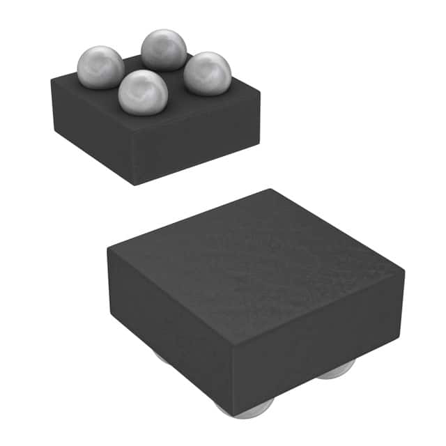
SN74AUP1G34YFPR is available in a small form factor package, such as a flip-chip package or a leadless package.
Essence
The essence of SN74AUP1G34YFPR lies in its ability to amplify and switch signals efficiently while consuming minimal power.
Packaging/Quantity
SN74AUP1G34YFPR is typically packaged in reels or tubes, with a quantity of 2500 units per reel/tube.
Specifications
- Supply Voltage: 0.8V to 3.6V
- Operating Temperature Range: -40°C to +85°C
- Input Voltage Range: 0V to VCC
- Output Voltage Range: 0V to VCC
- Maximum Propagation Delay: 2.5ns
- Maximum Quiescent Current: 10μA
Detailed Pin Configuration
SN74AUP1G34YFPR has the following pin configuration:
____
   A --|    |-- VCC
   B --|    |-- Y
 GND --|____|-- NC
Functional Features
- Single input (A) and single output (Y)
- Logic level translation capability
- High-speed signal switching
- Low power consumption
- Schmitt-trigger input for noise immunity
Advantages and Disadvantages
Advantages
- Low power consumption makes it suitable for battery-powered devices
- Wide operating voltage range allows compatibility with various systems
- Small package size saves board space
- High-speed operation enables efficient signal processing
Disadvantages
- Limited number of input/output pins restricts complex circuit designs
- Not suitable for high-power applications due to its low current handling capacity
Working Principles
SN74AUP1G34YFPR operates based on the principles of CMOS (Complementary Metal-Oxide-Semiconductor) technology. It utilizes a combination of p-type and n-type MOSFETs to amplify and switch signals. The Schmitt-trigger input ensures noise immunity by providing hysteresis.
Detailed Application Field Plans
SN74AUP1G34YFPR finds applications in various electronic devices, including but not limited to: - Mobile phones - Tablets - Digital cameras - Portable gaming consoles - Wearable devices
Detailed and Complete Alternative Models
Some alternative models that can be considered as alternatives to SN74AUP1G34YFPR are: - SN74LVC1G34DBVR - SN74HCT1G34DCKR - SN74LV1T34DBVR - SN74LVC1G34DCKR
These models offer similar functionality and characteristics, but may differ in terms of power consumption, speed, or package type.
In conclusion, SN74AUP1G34YFPR is a versatile integrated circuit that provides efficient signal amplification and switching capabilities. Its low power consumption, high-speed operation, and small package size make it suitable for a wide range of electronic devices. However, its limited pin count and low current handling capacity should be considered when designing complex circuits or high-power applications.
Seznam 10 běžných otázek a odpovědí souvisejících s aplikací SN74AUP1G34YFPR v technických řešeních
Sure! Here are 10 common questions and answers related to the application of SN74AUP1G34YFPR in technical solutions:
Q1: What is SN74AUP1G34YFPR? A1: SN74AUP1G34YFPR is a single buffer gate IC (integrated circuit) that provides high-performance voltage translation from a low-voltage (LVCMOS/LVTTL) input signal to a higher voltage level output.
Q2: What is the operating voltage range of SN74AUP1G34YFPR? A2: The operating voltage range for SN74AUP1G34YFPR is typically between 0.8V and 3.6V.
Q3: What is the maximum output current of SN74AUP1G34YFPR? A3: The maximum output current of SN74AUP1G34YFPR is typically around 32mA.
Q4: Can SN74AUP1G34YFPR be used for level shifting applications? A4: Yes, SN74AUP1G34YFPR is commonly used for level shifting applications where a low-voltage signal needs to be translated to a higher voltage level.
Q5: What is the propagation delay of SN74AUP1G34YFPR? A5: The propagation delay of SN74AUP1G34YFPR is typically around 1.7ns.
Q6: Is SN74AUP1G34YFPR suitable for high-speed applications? A6: Yes, SN74AUP1G34YFPR is designed for high-speed operation and can be used in various high-frequency applications.
Q7: Can SN74AUP1G34YFPR be used as a voltage level shifter for I2C communication? A7: Yes, SN74AUP1G34YFPR can be used as a voltage level shifter for I2C communication between devices operating at different voltage levels.
Q8: Does SN74AUP1G34YFPR have built-in ESD protection? A8: Yes, SN74AUP1G34YFPR is designed with built-in ESD (electrostatic discharge) protection to ensure robustness and reliability.
Q9: What is the package type of SN74AUP1G34YFPR? A9: SN74AUP1G34YFPR is available in a small footprint 5-pin SOT-23 package.
Q10: Can SN74AUP1G34YFPR be used in battery-powered applications? A10: Yes, SN74AUP1G34YFPR is suitable for battery-powered applications due to its low power consumption and wide operating voltage range.
Please note that the answers provided here are general and may vary depending on specific datasheet specifications and application requirements.