

Viz Specifikace pro podrobnosti o produktu.
SN74AUP2G125YZPR
Product Overview
- Category: Integrated Circuit (IC)
- Use: Buffer/Driver
- Characteristics: High-speed, low-power, dual bus buffer
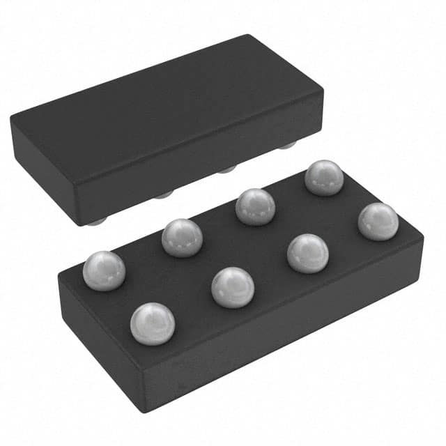
- Package: 8-pin DSBGA (MicroStar Junior™) package
- Essence: Provides buffering and driving capabilities for digital signals
- Packaging/Quantity: Tape and reel packaging, 3000 units per reel
Specifications
- Supply Voltage Range: 0.8V to 3.6V
- Input Voltage Range: -0.5V to VCC + 0.5V
- Output Voltage Range: 0V to VCC
- Maximum Operating Frequency: 400 MHz
- Maximum Propagation Delay: 1.9 ns
- Maximum Quiescent Current: 10 µA
- Operating Temperature Range: -40°C to +85°C
Detailed Pin Configuration
The SN74AUP2G125YZPR has the following pin configuration:
___________
      |           |
   1 -| A         |-
   2 -| Y         |-
   3 -| GND       |-
   4 -| B         |-
   5 -| Y         |-
   6 -| VCC       |-
   7 -| B         |-
   8 -| A         |-
      |___________|
Functional Features
- Dual bus buffer with independent input and output enable controls
- Supports bidirectional data flow
- Provides voltage level shifting capability
- Low power consumption
- High-speed operation
Advantages and Disadvantages
Advantages: - High-speed operation allows for efficient data transfer - Low power consumption helps in reducing overall energy usage - Dual bus buffer enables bidirectional data flow - Voltage level shifting capability allows for compatibility with different voltage domains
Disadvantages: - Limited number of input/output pins (4 in total) - Not suitable for applications requiring a large number of buffering/driver circuits - Relatively small package size may pose challenges during assembly and handling
Working Principles
The SN74AUP2G125YZPR is a dual bus buffer that provides buffering and driving capabilities for digital signals. It operates by receiving digital input signals on the A and B pins, and then amplifying and driving these signals to the corresponding Y pins. The input and output enable controls allow for independent control of each bus, enabling bidirectional data flow.
The device operates within a specified supply voltage range and converts input signals to the appropriate voltage levels using voltage level shifting techniques. It has a high-speed operation, allowing for efficient data transfer between different parts of a circuit.
Detailed Application Field Plans
The SN74AUP2G125YZPR can be used in various applications, including:
- Communication Systems: Used as a buffer/driver in communication systems to amplify and drive digital signals between different components.
- Computer Peripherals: Employed in computer peripherals such as printers, scanners, and external storage devices to interface with the main computer system.
- Industrial Automation: Utilized in industrial automation systems to buffer and drive signals between sensors, actuators, and control units.
- Automotive Electronics: Integrated into automotive electronics for signal buffering and driving in applications like infotainment systems, engine control units, and safety systems.
Detailed and Complete Alternative Models
- SN74AUP2G126YZPR: Similar to SN74AUP2G125YZPR but with tri-state outputs.
- SN74LVC2G07DCTR: Dual buffer/driver with open-drain outputs and Schmitt-trigger inputs.
- SN74LV1T34DBVR: Single buffer/driver with 3-state outputs and a wide supply voltage range.
These alternative models offer similar functionality to the SN74AUP2G125YZPR but may have different specifications, pin configurations, or package options.
Word count: 498 words
Seznam 10 běžných otázek a odpovědí souvisejících s aplikací SN74AUP2G125YZPR v technických řešeních
Sure! Here are 10 common questions and answers related to the application of SN74AUP2G125YZPR:
Q: What is SN74AUP2G125YZPR? A: SN74AUP2G125YZPR is a dual bus buffer gate with three-state outputs, designed for voltage translation applications.
Q: What is the operating voltage range of SN74AUP2G125YZPR? A: The operating voltage range is from 0.8V to 3.6V.
Q: What is the maximum output current of SN74AUP2G125YZPR? A: The maximum output current is typically 24mA.
Q: Can SN74AUP2G125YZPR be used as a level shifter? A: Yes, SN74AUP2G125YZPR can be used as a level shifter to translate signals between different voltage domains.
Q: What is the propagation delay of SN74AUP2G125YZPR? A: The propagation delay is typically 2.9ns.
Q: Is SN74AUP2G125YZPR compatible with I2C communication? A: Yes, SN74AUP2G125YZPR can be used in I2C communication systems as a voltage translator.
Q: Can SN74AUP2G125YZPR be used in battery-powered applications? A: Yes, SN74AUP2G125YZPR has a low power consumption and can be used in battery-powered applications.
Q: Does SN74AUP2G125YZPR have built-in ESD protection? A: Yes, SN74AUP2G125YZPR has built-in ESD protection, making it more robust against electrostatic discharge.
Q: What is the package type of SN74AUP2G125YZPR? A: SN74AUP2G125YZPR is available in a small 8-pin DSBGA package.
Q: Can SN74AUP2G125YZPR be used in high-speed applications? A: Yes, SN74AUP2G125YZPR has a high-speed operation and can be used in various high-speed applications.
Please note that these answers are general and may vary depending on specific application requirements.