

Viz Specifikace pro podrobnosti o produktu.
SN74CBTD3306CPWRG4
Product Overview
- Category: Integrated Circuit (IC)
- Use: Level Shifter and Bus Switch
- Characteristics: High-speed, low-power consumption
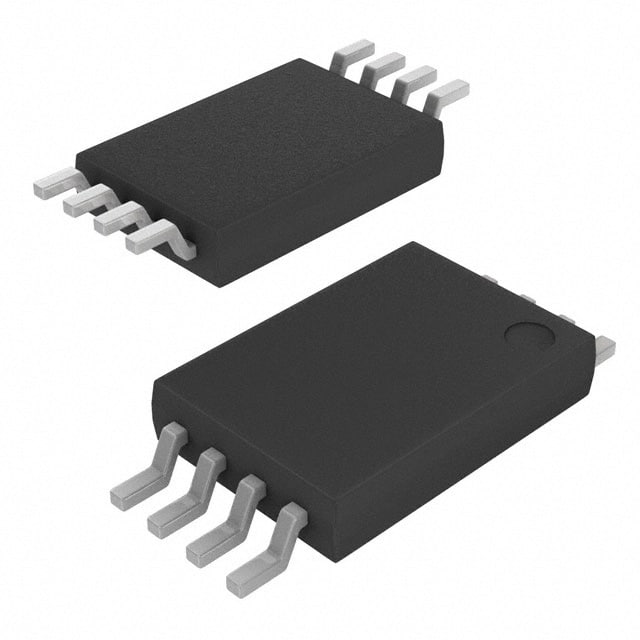
- Package: TSSOP-16
- Essence: Transceiver
- Packaging/Quantity: Tape and Reel, 2500 pieces per reel
Specifications
- Supply Voltage Range: 1.65V to 3.6V
- Logic Voltage Range: 1.65V to 5.5V
- Operating Temperature Range: -40°C to +85°C
- Input Capacitance: 2pF
- Output Capacitance: 3pF
- On-state Resistance: 5Ω
- Bandwidth: 100MHz
Detailed Pin Configuration
The SN74CBTD3306CPWRG4 has a total of 16 pins arranged as follows:
- OE (Output Enable)
- A1 (Control Input)
- B1 (Control Input)
- VCCA (Supply Voltage)
- GND (Ground)
- B2 (Control Input)
- A2 (Control Input)
- OE (Output Enable)
- Y1 (Output)
- Y2 (Output)
- VCCB (Supply Voltage)
- GND (Ground)
- Y3 (Output)
- Y4 (Output)
- A3 (Control Input)
- B3 (Control Input)
Functional Features
- Bidirectional level shifting between two voltage domains
- Low power consumption
- High-speed operation
- Wide supply voltage range
- ESD protection on all pins
Advantages and Disadvantages
Advantages: - Allows interfacing between different voltage levels - Supports bidirectional communication - Provides ESD protection for enhanced reliability - Compact package size for space-constrained applications
Disadvantages: - Limited to a maximum bandwidth of 100MHz - May require additional external components for specific applications
Working Principles
The SN74CBTD3306CPWRG4 is a level shifter and bus switch IC that enables bidirectional communication between two voltage domains. It utilizes a combination of MOSFETs and control logic to shift the voltage levels of input signals and route them to the appropriate output pins. The OE (Output Enable) pin controls the direction of data flow, allowing the user to enable or disable the outputs as needed.
Detailed Application Field Plans
The SN74CBTD3306CPWRG4 finds applications in various fields, including:
- Communication Systems: Enables voltage level translation between different communication protocols.
- Consumer Electronics: Facilitates interfacing between different voltage domains in devices such as smartphones, tablets, and gaming consoles.
- Industrial Automation: Allows seamless communication between different subsystems operating at different voltage levels.
- Automotive Electronics: Supports voltage level shifting in automotive systems, including infotainment, body control modules, and sensor interfaces.
Detailed and Complete Alternative Models
- SN74CBTD3306CDBQR: SOIC-16 package, same functionality as SN74CBTD3306CPWRG4.
- SN74CBTD3306CDR: SOIC-16 package, same functionality as SN74CBTD3306CPWRG4.
- SN74CBTD3306CPW: TSSOP-16 package, same functionality as SN74CBTD3306CPWRG4.
These alternative models offer similar features and performance characteristics, providing flexibility in choosing the most suitable option for specific design requirements.
In conclusion, the SN74CBTD3306CPWRG4 is a versatile level shifter and bus switch IC that enables bidirectional communication between different voltage domains. With its high-speed operation, low power consumption, and wide supply voltage range, it finds applications in various fields such as communication systems, consumer electronics, industrial automation, and automotive electronics. The IC's compact package size and availability of alternative models make it a popular choice for designers seeking efficient voltage level translation solutions.
Seznam 10 běžných otázek a odpovědí souvisejících s aplikací SN74CBTD3306CPWRG4 v technických řešeních
Sure! Here are 10 common questions and answers related to the application of SN74CBTD3306CPWRG4:
Q: What is SN74CBTD3306CPWRG4? A: SN74CBTD3306CPWRG4 is a high-speed, low-power digital switch designed for use in various technical solutions.
Q: What are the key features of SN74CBTD3306CPWRG4? A: Some key features include low on-state resistance, wide voltage range, low power consumption, and compatibility with various logic families.
Q: What is the maximum voltage that SN74CBTD3306CPWRG4 can handle? A: SN74CBTD3306CPWRG4 can handle a maximum voltage of up to 5.5V.
Q: Can SN74CBTD3306CPWRG4 be used as a bidirectional level shifter? A: Yes, SN74CBTD3306CPWRG4 can be used as a bidirectional level shifter for translating signals between different voltage domains.
Q: What is the typical operating frequency range of SN74CBTD3306CPWRG4? A: The typical operating frequency range of SN74CBTD3306CPWRG4 is from DC to 100 MHz.
Q: How many channels does SN74CBTD3306CPWRG4 have? A: SN74CBTD3306CPWRG4 has 10 channels, allowing it to switch multiple signals simultaneously.
Q: Is SN74CBTD3306CPWRG4 compatible with both CMOS and TTL logic levels? A: Yes, SN74CBTD3306CPWRG4 is compatible with both CMOS and TTL logic levels, making it versatile for various applications.
Q: Can SN74CBTD3306CPWRG4 be used in battery-powered devices? A: Yes, SN74CBTD3306CPWRG4 is designed to operate with low power consumption, making it suitable for battery-powered devices.
Q: What is the package type of SN74CBTD3306CPWRG4? A: SN74CBTD3306CPWRG4 comes in a TSSOP-20 package, which is compact and suitable for space-constrained designs.
Q: Are there any application notes or reference designs available for SN74CBTD3306CPWRG4? A: Yes, Texas Instruments provides application notes and reference designs that can help users understand and implement SN74CBTD3306CPWRG4 in their technical solutions.
Please note that these answers are general and may vary depending on specific requirements and use cases. It's always recommended to refer to the datasheet and consult with the manufacturer for detailed information.