Viz Specifikace pro podrobnosti o produktu.

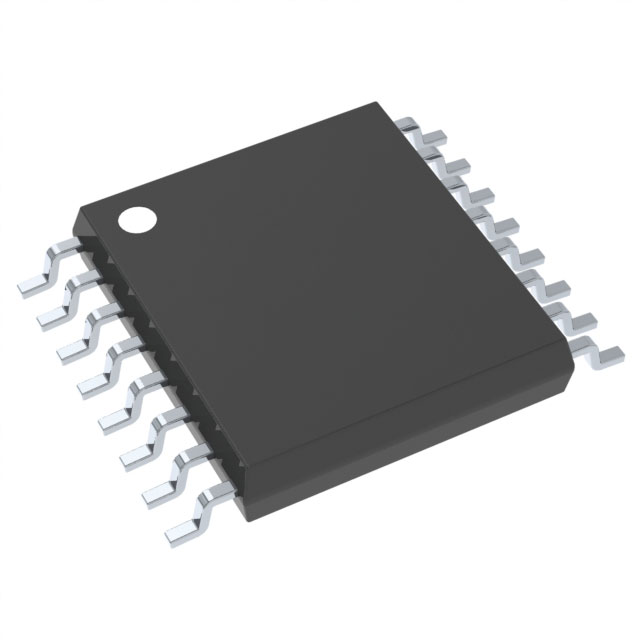
SN74HC251PWG4
Product Overview
Category: Integrated Circuit (IC)
Use: The SN74HC251PWG4 is a multiplexer/demultiplexer IC that allows for the selection of one of eight data inputs and routes it to a single output line. It is commonly used in digital systems where multiple data sources need to be selectively connected to a single destination.
Characteristics: - High-speed operation - Low power consumption - Wide operating voltage range - Schmitt-trigger inputs for noise immunity - 3-state outputs for easy bus interfacing
Package: TSSOP-16 (Thin Shrink Small Outline Package)
Essence: The SN74HC251PWG4 is designed to provide efficient data routing capabilities in various digital applications, ensuring reliable and accurate data transmission.
Packaging/Quantity: The SN74HC251PWG4 is typically available in reels or tubes, with a quantity of 2500 units per reel/tube.
Specifications
- Supply Voltage Range: 2V to 6V
- Input Voltage Range: 0V to VCC
- Output Voltage Range: 0V to VCC
- Operating Temperature Range: -40°C to +85°C
- Propagation Delay Time: 10 ns (max)
- Output Current: ±6 mA
- Input Capacitance: 3 pF (typ)
- Power Dissipation: 500 mW (max)
Pin Configuration
The SN74HC251PWG4 has a total of 16 pins arranged as follows:
___________
      |           |
   1  |1        16| VCC
   2  |2        15| A0
   3  |3        14| A1
   4  |4        13| A2
   5  |5        12| GND
   6  |6        11| Y
   7  |7        10| I0
   8  |8         9| I1
      |___________|
Functional Features
- Multiplexes or demultiplexes eight data inputs to a single output line.
- Selection of data input is controlled by the address inputs (A0, A1, A2).
- Output is in a high-impedance state when the enable input (G) is low.
- Schmitt-trigger inputs provide noise immunity and allow for reliable operation in noisy environments.
- 3-state outputs facilitate easy interfacing with other devices on a shared bus.
Advantages and Disadvantages
Advantages: - High-speed operation enables efficient data routing. - Low power consumption helps conserve energy in digital systems. - Wide operating voltage range allows for compatibility with various power supply levels. - Schmitt-trigger inputs ensure reliable operation in noisy environments. - 3-state outputs simplify bus interfacing.
Disadvantages: - Limited to eight data inputs and one output line, which may not be sufficient for certain complex applications. - Propagation delay time of 10 ns (max) may introduce latency in time-critical systems.
Working Principles
The SN74HC251PWG4 operates based on the principle of multiplexing and demultiplexing. It uses the address inputs (A0, A1, A2) to select one of the eight data inputs (I0-I7) and routes it to the output pin (Y). The enable input (G) controls the output state, allowing it to be either active or in a high-impedance state.
When the enable input is low, the output is in a high-impedance state, effectively disconnecting it from the data inputs. This feature enables multiple SN74HC251PWG4 ICs to be connected in parallel on a shared bus without causing conflicts.
The Schmitt-trigger inputs provide noise immunity by ensuring that the input signals are properly interpreted even in the presence of electrical noise or signal distortion.
Detailed Application Field Plans
The SN74HC251PWG4 finds applications in various digital systems where data routing and selection are required. Some specific application fields include:
- Data multiplexing in communication systems.
- Address decoding in microcontrollers and microprocessors.
- Input selection in audio/video equipment.
- Channel selection in remote control systems.
- Data routing in industrial automation systems.
Detailed and Complete Alternative Models
- CD74HC251E: Similar functionality with a different package (PDIP-16).
- MC74HC251N: Equivalent IC with a different manufacturer (Motorola).
These alternative models can be used as substitutes for the SN74HC251PWG4 based on specific requirements or availability.
In conclusion, the SN74HC251PWG4 is
Seznam 10 běžných otázek a odpovědí souvisejících s aplikací SN74HC251PWG4 v technických řešeních
Sure! Here are 10 common questions and answers related to the application of SN74HC251PWG4:
Q: What is SN74HC251PWG4? A: SN74HC251PWG4 is a multiplexer/demultiplexer IC (Integrated Circuit) that can be used in various technical solutions.
Q: What is the purpose of SN74HC251PWG4? A: SN74HC251PWG4 allows you to select one of multiple input signals and route it to a single output, or vice versa.
Q: What is the voltage range supported by SN74HC251PWG4? A: SN74HC251PWG4 supports a voltage range of 2V to 6V.
Q: How many inputs and outputs does SN74HC251PWG4 have? A: SN74HC251PWG4 has 8 inputs and 1 output.
Q: Can SN74HC251PWG4 be used as a demultiplexer? A: Yes, SN74HC251PWG4 can be used as both a multiplexer and a demultiplexer.
Q: What is the maximum operating frequency of SN74HC251PWG4? A: The maximum operating frequency of SN74HC251PWG4 is typically around 50 MHz.
Q: Does SN74HC251PWG4 have any built-in protection features? A: No, SN74HC251PWG4 does not have any built-in protection features. External protection circuitry may be required.
Q: Can SN74HC251PWG4 be cascaded to increase the number of inputs/outputs? A: Yes, SN74HC251PWG4 can be cascaded to increase the number of inputs/outputs by connecting the outputs of one IC to the inputs of another.
Q: What is the power supply voltage required for SN74HC251PWG4? A: SN74HC251PWG4 requires a power supply voltage of 2V to 6V.
Q: Can SN74HC251PWG4 be used in both digital and analog applications? A: SN74HC251PWG4 is primarily designed for digital applications, but it can also be used in some analog applications depending on the requirements.
Please note that these answers are general and may vary based on specific application requirements.

