

Viz Specifikace pro podrobnosti o produktu.
SN74LV244ADGVR
Product Overview
- Category: Integrated Circuit (IC)
- Use: Buffer/Line Driver
- Characteristics: Low-voltage, Octal Bus Buffer with 3-State Outputs
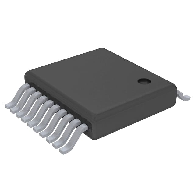
- Package: TSSOP-20
- Essence: This IC is designed to provide buffering and line driving capabilities for digital signals in low-voltage applications.
- Packaging/Quantity: Tape and Reel, 2500 units per reel
Specifications
- Supply Voltage Range: 1.65V to 5.5V
- Input Voltage Range: 0V to VCC
- Output Voltage Range: 0V to VCC
- High-Level Input Voltage: 0.7 x VCC
- Low-Level Input Voltage: 0.3 x VCC
- High-Level Output Voltage: 0.9 x VCC
- Low-Level Output Voltage: 0.1 x VCC
- Maximum Operating Frequency: 100MHz
- Number of Channels: 8
Detailed Pin Configuration
The SN74LV244ADGVR has a TSSOP-20 package with the following pin configuration:
- A1 - Input/Output
- Y1 - Output
- A2 - Input/Output
- Y2 - Output
- GND - Ground
- A3 - Input/Output
- Y3 - Output
- A4 - Input/Output
- Y4 - Output
- VCC - Power Supply
- OE - Output Enable
- Y5 - Output
- A5 - Input/Output
- Y6 - Output
- A6 - Input/Output
- Y7 - Output
- A7 - Input/Output
- Y8 - Output
- GND - Ground
- A8 - Input/Output
Functional Features
- Octal buffer with 3-state outputs
- Non-inverting outputs
- High-speed operation
- Low power consumption
- Supports bidirectional data flow
- Output enable (OE) pin for controlling the output state
Advantages and Disadvantages
Advantages: - Wide supply voltage range allows compatibility with various systems - High-speed operation enables efficient signal buffering - Low power consumption for energy-efficient applications - 3-state outputs provide flexibility in bus systems
Disadvantages: - Limited maximum operating frequency compared to some other ICs - TSSOP package may require careful handling during assembly
Working Principles
The SN74LV244ADGVR is an octal buffer IC that operates as a line driver for digital signals. It takes input signals from one or more sources and provides amplified, non-inverted output signals. The IC supports bidirectional data flow, allowing it to be used in both input and output applications.
The output enable (OE) pin controls the output state of the IC. When OE is low, the outputs are enabled and reflect the input signals. When OE is high, the outputs are in a high-impedance state, effectively disconnecting them from the bus.
Detailed Application Field Plans
The SN74LV244ADGVR is commonly used in various applications, including:
- Microcontroller interfacing: It can be used to interface microcontrollers with external devices, providing signal buffering and driving capabilities.
- Data communication systems: The IC can be employed in data communication systems to amplify and drive digital signals along transmission lines.
- Memory systems: It can be utilized in memory systems to buffer address and data lines, ensuring reliable communication between memory modules and controllers.
- Industrial automation: The IC finds application in industrial automation systems where it helps in buffering and driving control signals.
Detailed and Complete Alternative Models
- SN74LV244A: Similar to SN74LV244ADGVR but available in a different package (SOIC-20).
- SN74LVC244A: A similar IC with lower voltage operation (1.65V to 3.6V) and higher maximum operating frequency (125MHz).
- SN74HCT244: An alternative IC with TTL-compatible inputs and higher output drive capability.
These alternative models offer similar functionality and can be considered based on specific application requirements.
Word count: 510 words
Seznam 10 běžných otázek a odpovědí souvisejících s aplikací SN74LV244ADGVR v technických řešeních
Sure! Here are 10 common questions and answers related to the application of SN74LV244ADGVR:
Q: What is SN74LV244ADGVR? A: SN74LV244ADGVR is a specific type of integrated circuit (IC) known as a buffer/line driver. It is commonly used in digital systems to amplify and buffer signals.
Q: What is the voltage supply range for SN74LV244ADGVR? A: The voltage supply range for SN74LV244ADGVR is typically between 1.65V and 5.5V.
Q: What is the maximum output current of SN74LV244ADGVR? A: The maximum output current of SN74LV244ADGVR is typically around 12mA.
Q: Can SN74LV244ADGVR be used for bidirectional communication? A: No, SN74LV244ADGVR is a unidirectional buffer/line driver and cannot be used for bidirectional communication.
Q: What is the maximum operating frequency of SN74LV244ADGVR? A: The maximum operating frequency of SN74LV244ADGVR is typically around 100MHz.
Q: How many channels does SN74LV244ADGVR have? A: SN74LV244ADGVR has 8 channels, meaning it can buffer or amplify 8 different signals simultaneously.
Q: Can SN74LV244ADGVR handle both TTL and CMOS logic levels? A: Yes, SN74LV244ADGVR is compatible with both TTL and CMOS logic levels, making it versatile for various applications.
Q: What is the input voltage threshold for SN74LV244ADGVR? A: The input voltage threshold for SN74LV244ADGVR is typically around 0.8V.
Q: Can SN74LV244ADGVR be used in high-speed data transmission applications? A: Yes, SN74LV244ADGVR can be used in high-speed data transmission applications due to its fast propagation delay and high operating frequency.
Q: What is the package type of SN74LV244ADGVR? A: SN74LV244ADGVR comes in a small form factor package known as TSSOP-20, which stands for Thin Shrink Small Outline Package with 20 pins.
Please note that the answers provided here are general and may vary depending on specific datasheet specifications or application requirements.