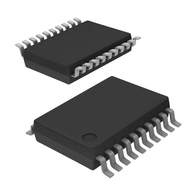
Viz Specifikace pro podrobnosti o produktu.

SN74LV573ATDBRE4
Product Overview
- Category: Integrated Circuit (IC)
- Use: Octal D-type transparent latch
- Characteristics:
- Low-voltage operation
- High-speed performance
- Transparent latch for easy data transfer
- Package: TSSOP (Thin Shrink Small Outline Package)
- Essence: This IC is designed to provide a convenient and efficient way of storing and transferring data in electronic circuits.
- Packaging/Quantity: Tape and reel, 2500 units per reel
Specifications
- Supply voltage range: 1.65V to 5.5V
- Input voltage range: 0V to VCC
- Output voltage range: 0V to VCC
- Operating temperature range: -40°C to +85°C
- Maximum clock frequency: 100MHz
- Number of inputs/outputs: 8
Detailed Pin Configuration
The SN74LV573ATDBRE4 has a total of 20 pins. The pin configuration is as follows:
- GND (Ground)
- D0 (Data input 0)
- D1 (Data input 1)
- D2 (Data input 2)
- D3 (Data input 3)
- D4 (Data input 4)
- D5 (Data input 5)
- D6 (Data input 6)
- D7 (Data input 7)
- OE (Output enable)
- CP (Clock pulse)
- LE (Latch enable)
- Q0 (Output 0)
- Q1 (Output 1)
- Q2 (Output 2)
- Q3 (Output 3)
- Q4 (Output 4)
- Q5 (Output 5)
- Q6 (Output 6)
- Q7 (Output 7)
Functional Features
- Octal D-type transparent latch with 3-state outputs
- Transparent latch allows data to be transferred when the latch enable (LE) signal is high
- Output enable (OE) signal controls the output state of the latch
- High-speed operation for efficient data transfer
- Low-voltage operation makes it suitable for battery-powered devices
Advantages and Disadvantages
Advantages: - Easy data transfer using the transparent latch - High-speed performance for quick data processing - Low-voltage operation extends battery life in portable devices
Disadvantages: - Limited number of inputs/outputs (8) - May require additional components for complex circuit designs
Working Principles
The SN74LV573ATDBRE4 operates based on the principles of digital logic. When the latch enable (LE) signal is high, the data inputs (D0-D7) are transferred to the outputs (Q0-Q7). The output enable (OE) signal controls whether the outputs are active or in a high-impedance state. This IC operates at low voltages, making it suitable for various electronic applications.
Detailed Application Field Plans
The SN74LV573ATDBRE4 can be used in a wide range of applications, including:
- Microcontrollers and microprocessors
- Data storage systems
- Communication devices
- Industrial automation
- Consumer electronics
- Automotive electronics
- Medical equipment
Detailed and Complete Alternative Models
- SN74LV573APWR - TSSOP package, 2500 units per reel
- SN74LV573ADGVR - TVSOP package, 3000 units per reel
- SN74LV573ANSR - SOP package, 2000 units per reel
- SN74LV573ARGYR - VQFN package, 4000 units per reel
- SN74LV573ADBRG4 - SSOP package, 3500 units per reel
These alternative models offer similar functionality and characteristics to the SN74LV573ATDBRE4, providing flexibility in design and availability options.
Word count: 410 words
Seznam 10 běžných otázek a odpovědí souvisejících s aplikací SN74LV573ATDBRE4 v technických řešeních
Sure! Here are 10 common questions and answers related to the application of SN74LV573ATDBRE4 in technical solutions:
Q: What is SN74LV573ATDBRE4? A: SN74LV573ATDBRE4 is a octal transparent D-type latch with 3-state outputs, designed for use as a storage element in a wide range of applications.
Q: What is the operating voltage range of SN74LV573ATDBRE4? A: The operating voltage range is from 1.65V to 5.5V.
Q: What is the maximum output current of SN74LV573ATDBRE4? A: The maximum output current is ±32mA.
Q: Can SN74LV573ATDBRE4 be used in both parallel and serial data transfer applications? A: Yes, SN74LV573ATDBRE4 can be used in both parallel and serial data transfer applications.
Q: What is the maximum clock frequency supported by SN74LV573ATDBRE4? A: The maximum clock frequency supported is 100MHz.
Q: Does SN74LV573ATDBRE4 have an internal pull-up or pull-down resistor? A: No, SN74LV573ATDBRE4 does not have an internal pull-up or pull-down resistor.
Q: Can SN74LV573ATDBRE4 be used in high-speed applications? A: Yes, SN74LV573ATDBRE4 is designed for high-speed operation and can be used in high-speed applications.
Q: What is the power supply voltage range for SN74LV573ATDBRE4? A: The power supply voltage range is from 1.65V to 5.5V.
Q: Can SN74LV573ATDBRE4 be used in both CMOS and TTL logic level applications? A: Yes, SN74LV573ATDBRE4 is compatible with both CMOS and TTL logic levels.
Q: What is the package type of SN74LV573ATDBRE4? A: SN74LV573ATDBRE4 is available in a TSSOP-20 package.
Please note that these answers are general and may vary depending on the specific application and requirements. It is always recommended to refer to the datasheet and consult the manufacturer for detailed information.

