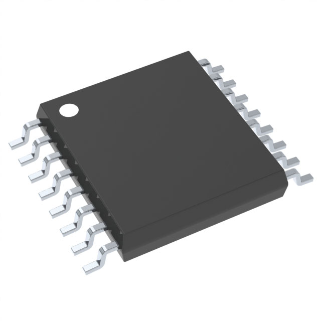
Viz Specifikace pro podrobnosti o produktu.

SN74LV595AIPWRQ1
Product Overview
Category
SN74LV595AIPWRQ1 belongs to the category of integrated circuits (ICs).
Use
This IC is commonly used as a shift register and output latch in various electronic devices.
Characteristics
- Low-voltage operation
- Wide operating temperature range
- High-speed data transfer
- Serial-to-parallel conversion capability
Package
SN74LV595AIPWRQ1 is available in a small-sized TSSOP package.
Essence
The essence of SN74LV595AIPWRQ1 lies in its ability to efficiently control multiple outputs using a minimal number of pins.
Packaging/Quantity
This IC is typically packaged in reels, with each reel containing a specific quantity of units. The exact quantity may vary depending on the manufacturer.
Specifications
- Supply Voltage: 2V to 5.5V
- Operating Temperature Range: -40°C to +125°C
- Maximum Clock Frequency: 100 MHz
- Number of Output Pins: 8
- Serial Data Input Pin: 1
- Serial Data Output Pin: 1
- Shift Register Length: 8 bits
Detailed Pin Configuration
- VCC: Power supply voltage input
- GND: Ground reference
- SER: Serial data input
- SRCLK: Shift register clock input
- RCLK: Output latch clock input
- OE: Output enable
- QH' (SER OUT): Serial data output
- QA-QH: Parallel output pins
Functional Features
- Serial-to-parallel conversion: Allows serial data to be converted into parallel data for controlling multiple outputs.
- Output latch: Provides the ability to store and hold the output values until updated.
- Cascade capability: Multiple SN74LV595AIPWRQ1 ICs can be connected in series to expand the number of outputs.
Advantages and Disadvantages
Advantages
- Low-voltage operation makes it suitable for battery-powered devices.
- High-speed data transfer enables efficient control of outputs.
- Small package size saves board space.
- Cascade capability allows for scalability.
Disadvantages
- Limited number of output pins (8) may not be sufficient for complex applications.
- Lack of built-in protection features against voltage spikes or ESD events.
Working Principles
SN74LV595AIPWRQ1 operates based on a shift register and latch mechanism. The serial data input (SER) is shifted through the shift register on each rising edge of the shift register clock (SRCLK). The output latch clock (RCLK) is used to update the parallel outputs with the values stored in the shift register. The output enable (OE) pin controls whether the outputs are active or in a high-impedance state.
Detailed Application Field Plans
SN74LV595AIPWRQ1 finds applications in various fields, including but not limited to: - LED matrix displays - Seven-segment displays - Motor control circuits - Data storage systems - Communication devices
Detailed and Complete Alternative Models
Some alternative models that offer similar functionality to SN74LV595AIPWRQ1 include: - 74HC595 - CD4094 - TPIC6B595 - STP16C596
These alternatives may have slight differences in specifications and pin configurations, so it is important to refer to their respective datasheets for detailed information.
Word count: 410
Seznam 10 běžných otázek a odpovědí souvisejících s aplikací SN74LV595AIPWRQ1 v technických řešeních
Sure! Here are 10 common questions and answers related to the application of SN74LV595AIPWRQ1 in technical solutions:
1. What is the SN74LV595AIPWRQ1? - The SN74LV595AIPWRQ1 is a shift register and storage register with 8-bit parallel-in, serial-out capability.
2. What is the operating voltage range of SN74LV595AIPWRQ1? - The operating voltage range of SN74LV595AIPWRQ1 is from 2 V to 5.5 V.
3. How many output pins does SN74LV595AIPWRQ1 have? - SN74LV595AIPWRQ1 has 8 output pins.
4. Can I cascade multiple SN74LV595AIPWRQ1 devices together? - Yes, you can cascade multiple SN74LV595AIPWRQ1 devices together to expand the number of outputs.
5. What is the maximum clock frequency supported by SN74LV595AIPWRQ1? - The maximum clock frequency supported by SN74LV595AIPWRQ1 is 33 MHz.
6. How do I control the data input to SN74LV595AIPWRQ1? - You can control the data input by shifting in the desired data through the serial input pin (SER).
7. Can I use SN74LV595AIPWRQ1 for driving LEDs? - Yes, SN74LV595AIPWRQ1 is commonly used for driving LEDs as it can sink up to 20 mA per output pin.
8. Does SN74LV595AIPWRQ1 have any built-in protection features? - Yes, SN74LV595AIPWRQ1 has built-in thermal shutdown and overvoltage protection features.
9. What is the package type of SN74LV595AIPWRQ1? - SN74LV595AIPWRQ1 comes in a TSSOP-16 package.
10. Can I use SN74LV595AIPWRQ1 in automotive applications? - Yes, SN74LV595AIPWRQ1 is specifically designed for automotive applications and is qualified to AEC-Q100 standards.
Please note that these answers are general and may vary depending on the specific application and requirements.

