

Viz Specifikace pro podrobnosti o produktu.
SN74LV74ADGVR
Product Overview
- Category: Integrated Circuit (IC)
- Use: Flip-Flop
- Characteristics: Low-voltage, dual D-type positive-edge-triggered flip-flop
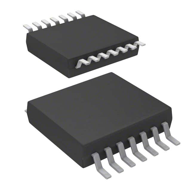
- Package: VSSOP (Very Small Outline Package)
- Essence: Digital logic component for storing and manipulating binary data
- Packaging/Quantity: Tape and reel, 2500 units per reel
Specifications
- Supply Voltage Range: 1.65V to 5.5V
- High-Level Input Voltage: 2V (minimum), 5.5V (maximum)
- Low-Level Input Voltage: -0.3V (minimum), 0.8V (maximum)
- High-Level Output Voltage: 2.4V (minimum), VCC (maximum)
- Low-Level Output Voltage: 0V (minimum), 0.4V (maximum)
- Maximum Operating Frequency: 125MHz
- Propagation Delay Time: 7.6ns (typical)
Detailed Pin Configuration
The SN74LV74ADGVR has a total of 14 pins:
- CLR (Clear) - Active low clear input
- D (Data) - Data input
- CLK (Clock) - Clock input
- PR (Preset) - Active low preset input
- Q (Output) - Complementary output
- Q̅ (Output) - Non-complementary output
- GND (Ground) - Ground reference
- Q̅ (Output) - Non-complementary output
- Q (Output) - Complementary output
- VCC (Supply Voltage) - Positive power supply
- D (Data) - Data input
- CLK (Clock) - Clock input
- PR (Preset) - Active low preset input
- CLR (Clear) - Active low clear input
Functional Features
- Dual D-type positive-edge-triggered flip-flop
- Low-voltage operation suitable for battery-powered devices
- High-speed operation with a maximum frequency of 125MHz
- Clear and preset inputs for synchronous reset functionality
- Complementary and non-complementary outputs for flexible data manipulation
Advantages and Disadvantages
Advantages: - Low-voltage operation allows for compatibility with various systems - High-speed operation enables efficient data processing - Synchronous reset functionality provides reliable control over the flip-flop state - Small package size saves board space in compact designs
Disadvantages: - Limited supply voltage range may restrict certain applications - Propagation delay time may affect timing-sensitive operations
Working Principles
The SN74LV74ADGVR is a dual D-type positive-edge-triggered flip-flop. It stores binary data using two D inputs and transfers it to the complementary and non-complementary outputs on the rising edge of the clock signal. The clear and preset inputs allow for synchronous reset, ensuring predictable initial states. The low-voltage operation makes it suitable for battery-powered devices.
Detailed Application Field Plans
The SN74LV74ADGVR is commonly used in various digital systems, including:
- Microcontrollers and microprocessors
- Communication systems
- Data storage devices
- Industrial automation equipment
- Consumer electronics
Its ability to store and manipulate binary data makes it essential in these applications, enabling tasks such as data synchronization, state control, and sequential logic implementation.
Detailed and Complete Alternative Models
- SN74LV74ADR - SOIC (Small Outline Integrated Circuit) package variant
- SN74LV74APWR - TSSOP (Thin Shrink Small Outline Package) package variant
- SN74LV74ANSR - SOP (Small Outline Package) package variant
- SN74LV74ARGYR - QFN (Quad Flat No-leads) package variant
These alternative models offer similar functionality and characteristics, providing flexibility in choosing the most suitable package for specific design requirements.
Word count: 445 words
Seznam 10 běžných otázek a odpovědí souvisejících s aplikací SN74LV74ADGVR v technických řešeních
Sure! Here are 10 common questions and answers related to the application of SN74LV74ADGVR:
Q: What is the SN74LV74ADGVR? A: The SN74LV74ADGVR is a dual positive-edge-triggered D-type flip-flop integrated circuit (IC) that can be used in various digital logic applications.
Q: What is the operating voltage range of SN74LV74ADGVR? A: The operating voltage range of SN74LV74ADGVR is from 1.65V to 5.5V.
Q: What is the maximum clock frequency supported by SN74LV74ADGVR? A: The maximum clock frequency supported by SN74LV74ADGVR is typically around 125 MHz.
Q: How many flip-flops are there in SN74LV74ADGVR? A: SN74LV74ADGVR contains two independent D-type flip-flops.
Q: What is the output drive capability of SN74LV74ADGVR? A: The output drive capability of SN74LV74ADGVR is typically 8 mA.
Q: Can SN74LV74ADGVR be used in both synchronous and asynchronous applications? A: Yes, SN74LV74ADGVR can be used in both synchronous and asynchronous applications.
Q: What is the setup time requirement for the data input signal? A: The setup time requirement for the data input signal is typically 100 ns.
Q: Does SN74LV74ADGVR have any power-saving features? A: Yes, SN74LV74ADGVR has a power-down mode that reduces power consumption when not in use.
Q: What is the typical propagation delay of SN74LV74ADGVR? A: The typical propagation delay of SN74LV74ADGVR is around 5 ns.
Q: Can SN74LV74ADGVR be used in high-speed applications? A: Yes, SN74LV74ADGVR can be used in high-speed applications due to its low propagation delay and high clock frequency support.
Please note that these answers are general and may vary depending on specific datasheet specifications.