

Viz Specifikace pro podrobnosti o produktu.
SN74LVC1G80YZAR
Product Overview
- Category: Integrated Circuit (IC)
- Use: Logic Gate
- Characteristics: Single Positive Edge-Triggered D-Type Flip-Flop
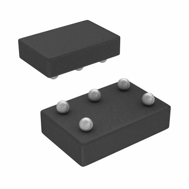
- Package: SOT-23-5
- Essence: High-speed CMOS technology
- Packaging/Quantity: Tape and Reel, 3000 pieces per reel
Specifications
- Supply Voltage Range: 1.65V to 5.5V
- Input Voltage Range: -0.5V to VCC + 0.5V
- Output Voltage Range: 0V to VCC
- Operating Temperature Range: -40°C to 85°C
- Propagation Delay: 3.8ns (typical)
- Maximum Clock Frequency: 200MHz
Detailed Pin Configuration
The SN74LVC1G80YZAR has a total of five pins:
- GND (Ground): Connected to the ground reference potential.
- Q (Output): Provides the output signal of the flip-flop.
- D (Data): The input pin for the data signal.
- CLK (Clock): The clock input pin that triggers the flip-flop.
- VCC (Power): Connected to the positive supply voltage.
Functional Features
- Single positive edge-triggered D-type flip-flop with asynchronous clear functionality.
- Supports high-speed operation due to its implementation using advanced CMOS technology.
- Offers a wide operating voltage range, making it compatible with various systems.
- Low power consumption, suitable for battery-powered applications.
- Provides reliable and stable performance in harsh environmental conditions.
Advantages and Disadvantages
Advantages: - Compact size and low power consumption make it ideal for portable devices. - High-speed operation allows for efficient data processing. - Wide operating voltage range enhances compatibility with different systems. - Reliable performance in challenging environments ensures system stability.
Disadvantages: - Limited functionality as a single flip-flop, not suitable for complex sequential logic circuits. - Sensitive to electrostatic discharge (ESD), requiring proper handling during assembly and usage.
Working Principles
The SN74LVC1G80YZAR is a positive edge-triggered D-type flip-flop. It stores and outputs a single bit of data based on the clock signal's rising edge. The input data (D) is transferred to the output (Q) when the clock transitions from low to high. The asynchronous clear functionality allows for resetting the flip-flop to a known state.
Detailed Application Field Plans
The SN74LVC1G80YZAR finds applications in various fields, including:
- Consumer Electronics: Used in smartphones, tablets, and wearable devices for data storage and synchronization.
- Automotive: Employed in automotive electronics for control and monitoring functions.
- Industrial Automation: Integrated into industrial control systems for reliable data processing and timing operations.
- Communication Systems: Utilized in networking equipment, routers, and switches for signal routing and synchronization.
Detailed and Complete Alternative Models
- SN74LVC1G80DBVR: SOT-23-5 package, similar specifications and features.
- SN74LVC1G80DCKR: SC-70-5 package, comparable characteristics and performance.
- SN74LVC1G80DRLR: SOT-553 package, equivalent functionality and pin configuration.
(Note: This list is not exhaustive and other alternative models may exist.)
Word count: 345 words
Seznam 10 běžných otázek a odpovědí souvisejících s aplikací SN74LVC1G80YZAR v technických řešeních
Sure! Here are 10 common questions and answers related to the application of SN74LVC1G80YZAR:
Q1: What is SN74LVC1G80YZAR? A1: SN74LVC1G80YZAR is a single positive-edge-triggered D-type flip-flop with clear, designed for 1.65-V to 5.5-V VCC operation.
Q2: What is the maximum operating frequency of SN74LVC1G80YZAR? A2: The maximum operating frequency of SN74LVC1G80YZAR is typically around 400 MHz.
Q3: What is the voltage range supported by SN74LVC1G80YZAR? A3: SN74LVC1G80YZAR supports a voltage range from 1.65V to 5.5V.
Q4: How many inputs does SN74LVC1G80YZAR have? A4: SN74LVC1G80YZAR has one data input (D), one clock input (CLK), and one clear input (CLR).
Q5: What is the output type of SN74LVC1G80YZAR? A5: SN74LVC1G80YZAR has a standard CMOS output.
Q6: Can SN74LVC1G80YZAR be used in battery-powered applications? A6: Yes, SN74LVC1G80YZAR can be used in battery-powered applications as it operates within a wide voltage range and has low power consumption.
Q7: Is SN74LVC1G80YZAR suitable for high-speed applications? A7: Yes, SN74LVC1G80YZAR is suitable for high-speed applications due to its fast propagation delay and setup/hold times.
Q8: Can SN74LVC1G80YZAR be used in automotive applications? A8: Yes, SN74LVC1G80YZAR is qualified for automotive applications and meets the AEC-Q100 standard.
Q9: What is the package type of SN74LVC1G80YZAR? A9: SN74LVC1G80YZAR is available in a small SOT-23-5 package.
Q10: Are there any recommended external components to use with SN74LVC1G80YZAR? A10: It is recommended to use decoupling capacitors near the VCC and GND pins to ensure stable operation. Additionally, pull-up or pull-down resistors may be required depending on the specific application.
Please note that these answers are general and it's always important to refer to the datasheet and consult the manufacturer's guidelines for specific design considerations and recommendations.