

Viz Specifikace pro podrobnosti o produktu.
SN74LVC2G17YEPR
Basic Information Overview
- Category: Integrated Circuit (IC)
- Use: Logic Gate
- Characteristics: Dual Schmitt-Trigger Buffer/Driver
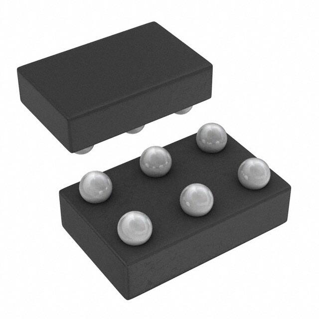
- Package: 8-pin VSSOP (Very Small Outline Package)
- Essence: High-speed CMOS technology
- Packaging/Quantity: Tape and Reel, 2500 units per reel
Specifications
- Supply Voltage Range: 1.65V to 5.5V
- Input Voltage Range: 0V to VCC
- Output Voltage Range: 0V to VCC
- Maximum Operating Frequency: 100 MHz
- Propagation Delay: 3.6 ns (typical)
- Input Capacitance: 3 pF (typical)
- Output Current: ±24 mA
Detailed Pin Configuration
The SN74LVC2G17YEPR has the following pin configuration:
___________
   1 -| A         |-
   2 -| Y         |-
   3 -| GND       |-
   4 -| B         |-
   5 -| Y         |-
   6 -| VCC       |-
   7 -| NC        |-
   8 -| GND       |-
       -----------
Functional Features
- Dual Schmitt-trigger buffer/driver with open-drain outputs
- Provides signal buffering and level shifting capabilities
- Schmitt-trigger inputs allow for hysteresis and noise immunity
- Supports bidirectional communication between different voltage domains
Advantages and Disadvantages
Advantages: - Wide supply voltage range allows compatibility with various systems - High-speed operation enables efficient data transmission - Schmitt-trigger inputs enhance noise immunity and signal integrity - Open-drain outputs facilitate flexible interfacing
Disadvantages: - Limited output current may restrict use in high-current applications - 8-pin package may limit the number of I/Os in a single IC
Working Principles
The SN74LVC2G17YEPR is a dual Schmitt-trigger buffer/driver that operates using high-speed CMOS technology. It provides signal buffering and level shifting capabilities, making it suitable for interfacing between different voltage domains. The Schmitt-trigger inputs ensure hysteresis and noise immunity, allowing reliable operation even in noisy environments. The open-drain outputs enable flexible connection to other devices.
Detailed Application Field Plans
The SN74LVC2G17YEPR can be used in various applications, including but not limited to: 1. Communication systems: Signal buffering and level shifting in UART, SPI, or I2C interfaces. 2. Industrial automation: Interfacing between different voltage levels in control systems. 3. Automotive electronics: Level translation between microcontrollers and sensors/actuators. 4. Consumer electronics: Signal conditioning and level shifting in audio/video interfaces. 5. IoT devices: Voltage level adaptation in sensor networks and communication modules.
Detailed and Complete Alternative Models
Some alternative models that offer similar functionality to the SN74LVC2G17YEPR are: 1. NC7SZ17P6X by Fairchild Semiconductor 2. TC7SZ17FU by Toshiba Semiconductor 3. MC74VHC1GT17 by ON Semiconductor 4. 74LVC2G17 by NXP Semiconductors 5. SN74LVC2G17DBVR by Texas Instruments
(Note: These alternative models may have slight variations in specifications and pin configuration. Refer to respective datasheets for detailed information.)
Word count: 400 words
Seznam 10 běžných otázek a odpovědí souvisejících s aplikací SN74LVC2G17YEPR v technických řešeních
Sure! Here are 10 common questions and answers related to the application of SN74LVC2G17YEPR in technical solutions:
Q: What is SN74LVC2G17YEPR? A: SN74LVC2G17YEPR is a dual Schmitt-trigger buffer/driver integrated circuit (IC) that can be used for signal conditioning and level shifting applications.
Q: What is the operating voltage range of SN74LVC2G17YEPR? A: The operating voltage range of SN74LVC2G17YEPR is from 1.65V to 5.5V.
Q: What is the maximum output current of SN74LVC2G17YEPR? A: The maximum output current of SN74LVC2G17YEPR is typically 32mA.
Q: Can SN74LVC2G17YEPR be used as a level shifter? A: Yes, SN74LVC2G17YEPR can be used as a level shifter to convert signals between different voltage levels.
Q: Does SN74LVC2G17YEPR have Schmitt-trigger inputs? A: Yes, SN74LVC2G17YEPR has Schmitt-trigger inputs, which provide hysteresis and improve noise immunity.
Q: What is the propagation delay of SN74LVC2G17YEPR? A: The propagation delay of SN74LVC2G17YEPR is typically around 4.8ns.
Q: Can SN74LVC2G17YEPR drive capacitive loads? A: Yes, SN74LVC2G17YEPR can drive capacitive loads up to 50pF.
Q: Is SN74LVC2G17YEPR suitable for high-speed applications? A: Yes, SN74LVC2G17YEPR is designed for high-speed operation and can be used in applications with fast switching requirements.
Q: Can SN74LVC2G17YEPR be used in battery-powered devices? A: Yes, SN74LVC2G17YEPR has a wide operating voltage range and low power consumption, making it suitable for battery-powered devices.
Q: What package options are available for SN74LVC2G17YEPR? A: SN74LVC2G17YEPR is available in various package options, such as SOT-23 and VSSOP, providing flexibility for different PCB layouts and space constraints.
Please note that the answers provided here are general and may vary depending on specific datasheet specifications and application requirements.