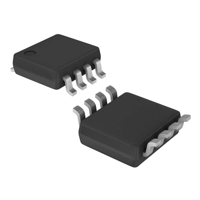
Viz Specifikace pro podrobnosti o produktu.

SN74LVC3G07DCUTE4
Basic Information Overview
- Category: Integrated Circuit (IC)
- Use: Logic Gate Buffer/Driver
- Characteristics:
- Low-voltage CMOS technology
- Triple buffer/driver with open-drain outputs
- Wide operating voltage range: 1.65V to 5.5V
- High-speed operation: up to 100 MHz
- Package: SOT-23-6
- Essence: The SN74LVC3G07DCUTE4 is a versatile logic gate buffer/driver that provides high-speed signal buffering and driving capabilities in various electronic applications.
- Packaging/Quantity: Available in tape and reel packaging, with 3000 units per reel.
Specifications
- Supply Voltage Range: 1.65V to 5.5V
- Input Voltage Range: 0V to VCC
- Output Voltage Range: 0V to VCC
- Operating Temperature Range: -40°C to +85°C
- Propagation Delay: 2.7 ns (typical)
- Output Current: ±32 mA
- Input Capacitance: 3 pF (typical)
- Output Capacitance: 5 pF (typical)
Detailed Pin Configuration
The SN74LVC3G07DCUTE4 has a total of six pins arranged as follows:
___________
      |           |
   1 -| A         |
   2 -| Y         |
   3 -| GND       |
   4 -| Y         |
   5 -| B         |
   6 -| VCC       |
      |___________|
Functional Features
- Triple Buffer/Driver: The IC features three independent buffer/driver circuits, allowing it to handle multiple input signals simultaneously.
- Open-Drain Outputs: The outputs are designed as open-drain, which means they can be connected to other devices or circuits without causing conflicts in voltage levels.
- High-Speed Operation: With a maximum operating frequency of 100 MHz, the SN74LVC3G07DCUTE4 is suitable for applications requiring fast signal propagation.
Advantages and Disadvantages
Advantages: - Wide operating voltage range enables compatibility with various power supply systems. - Low-voltage CMOS technology provides low power consumption and improved noise immunity. - Small package size (SOT-23-6) allows for space-efficient circuit designs.
Disadvantages: - Limited output current may restrict its use in high-current applications. - Lack of built-in protection features against overvoltage or ESD events.
Working Principles
The SN74LVC3G07DCUTE4 operates based on CMOS technology, utilizing MOSFET transistors to control the flow of current. When an input signal is applied to one of the buffer/driver inputs (A or B), the IC amplifies and buffers the signal, driving it to the corresponding output pin (Y). The open-drain configuration ensures that the output voltage level is determined by external pull-up resistors.
Detailed Application Field Plans
The SN74LVC3G07DCUTE4 finds applications in various electronic systems, including but not limited to: 1. Communication Systems: Used for signal buffering and driving in data transmission circuits. 2. Industrial Control Systems: Employed in control logic circuits to interface between different voltage levels. 3. Automotive Electronics: Suitable for driving LEDs, sensors, and other peripheral devices in automotive applications. 4. Consumer Electronics: Integrated into audio/video equipment, gaming consoles, and portable devices for signal conditioning and level shifting.
Detailed and Complete Alternative Models
- SN74LVC3G17DCUR: Similar triple buffer/driver IC with Schmitt-trigger inputs.
- SN74LVC3G34DCUR: Triple buffer/driver IC with non-inverting outputs and Schmitt-trigger inputs.
- SN74LVC3G04DCUR: Triple inverter IC with open-drain outputs.
These alternative models offer similar functionality and can be considered as substitutes for the SN74LVC3G07DCUTE4 in different applications.
Word count: 512 words
Seznam 10 běžných otázek a odpovědí souvisejících s aplikací SN74LVC3G07DCUTE4 v technických řešeních
Sure! Here are 10 common questions and answers related to the application of SN74LVC3G07DCUTE4 in technical solutions:
Q: What is SN74LVC3G07DCUTE4? A: SN74LVC3G07DCUTE4 is a triple buffer gate with open-drain outputs, commonly used in digital logic applications.
Q: What is the voltage range supported by SN74LVC3G07DCUTE4? A: SN74LVC3G07DCUTE4 supports a voltage range from 1.65V to 5.5V.
Q: How many buffers are there in SN74LVC3G07DCUTE4? A: SN74LVC3G07DCUTE4 has three independent buffer gates.
Q: What is the maximum output current of SN74LVC3G07DCUTE4? A: The maximum output current of SN74LVC3G07DCUTE4 is typically 32mA.
Q: Can SN74LVC3G07DCUTE4 be used for level shifting between different voltage domains? A: Yes, SN74LVC3G07DCUTE4 can be used for level shifting between voltage domains due to its wide voltage range support.
Q: Is SN74LVC3G07DCUTE4 suitable for bidirectional communication? A: No, SN74LVC3G07DCUTE4 is not bidirectional. It only supports unidirectional signal buffering.
Q: What is the propagation delay of SN74LVC3G07DCUTE4? A: The typical propagation delay of SN74LVC3G07DCUTE4 is around 3.8ns.
Q: Can SN74LVC3G07DCUTE4 be used in high-speed applications? A: Yes, SN74LVC3G07DCUTE4 is designed for high-speed operation and can be used in such applications.
Q: Does SN74LVC3G07DCUTE4 have built-in ESD protection? A: Yes, SN74LVC3G07DCUTE4 has built-in ESD protection to safeguard against electrostatic discharge.
Q: What package options are available for SN74LVC3G07DCUTE4? A: SN74LVC3G07DCUTE4 is available in a small SOT-23-6 package, which is commonly used for surface-mount applications.
Please note that the answers provided here are general and may vary depending on specific datasheet specifications and application requirements.

