

Viz Specifikace pro podrobnosti o produktu.
SN74LVC574ARGYR
Product Overview
- Category: Integrated Circuit
- Use: Flip-Flop / Latch
- Characteristics: Low Voltage, CMOS Technology
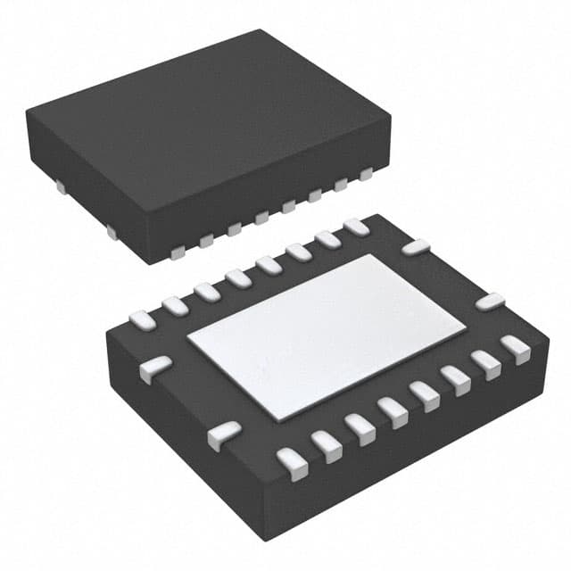
- Package: VQFN-20
- Essence: Octal D-Type Flip-Flop with 3-State Outputs
- Packaging/Quantity: Tape and Reel, 2500 pieces per reel
Specifications
The SN74LVC574ARGYR is an octal D-type flip-flop with 3-state outputs. It operates at low voltage levels and utilizes CMOS technology. The integrated circuit comes in a VQFN-20 package and is available in tape and reel packaging with 2500 pieces per reel.
Detailed Pin Configuration
The SN74LVC574ARGYR has a total of 20 pins. The pin configuration is as follows:
- Pin 1: Output 0 (Q0)
- Pin 2: Output 1 (Q1)
- Pin 3: Output 2 (Q2)
- Pin 4: Output 3 (Q3)
- Pin 5: Output 4 (Q4)
- Pin 6: Output 5 (Q5)
- Pin 7: Output 6 (Q6)
- Pin 8: Output 7 (Q7)
- Pin 9: GND (Ground)
- Pin 10: D0 (Data Input 0)
- Pin 11: D1 (Data Input 1)
- Pin 12: D2 (Data Input 2)
- Pin 13: D3 (Data Input 3)
- Pin 14: D4 (Data Input 4)
- Pin 15: D5 (Data Input 5)
- Pin 16: D6 (Data Input 6)
- Pin 17: D7 (Data Input 7)
- Pin 18: CLK (Clock Input)
- Pin 19: OE (Output Enable)
- Pin 20: VCC (Power Supply)
Functional Features
The SN74LVC574ARGYR is designed to store and transfer data in electronic systems. It features eight flip-flops with 3-state outputs, allowing for efficient data storage and retrieval. The device operates at low voltage levels, making it suitable for battery-powered applications. The CMOS technology used ensures low power consumption and high noise immunity.
Advantages and Disadvantages
Advantages: - Low voltage operation - CMOS technology for low power consumption - 3-state outputs for efficient data transfer - High noise immunity
Disadvantages: - Limited number of flip-flops (8) - Not suitable for high-speed applications
Working Principles
The SN74LVC574ARGYR operates based on the principles of flip-flops and latch circuits. It stores and transfers data using D-type flip-flops, which are controlled by clock signals. When the clock input (CLK) transitions from low to high, the data present at the D-inputs is transferred to the corresponding Q-outputs. The output enable (OE) pin controls the 3-state outputs, allowing them to be either active or in a high-impedance state.
Detailed Application Field Plans
The SN74LVC574ARGYR can be used in various applications that require data storage and transfer. Some potential application fields include:
- Microcontrollers: The IC can be used to store and retrieve data in microcontroller-based systems, enabling efficient data processing and control.
- Communication Systems: It can be utilized in communication systems for buffering and transferring data between different components, ensuring reliable data transmission.
- Industrial Automation: The IC can be employed in industrial automation systems for storing and transferring control signals, enabling precise and efficient control of machinery and processes.
- Automotive Electronics: It can be integrated into automotive electronics for data storage and transfer, facilitating various functions such as sensor data processing and control signal generation.
Detailed and Complete Alternative Models
- SN74LVC574APWR
- SN74LVC574ADBR
- SN74LVC574ADGVR
- SN74LVC574ADGVRE4
- SN74LVC574ADGVRG4
- SN74LVC574ADGVRG4-EP
- SN74LVC574ADGVRG4Q1
- SN74LVC574ADGVRG4Q1E3
- SN74LVC574ADGVRG4Q1E3A
- SN74LVC574ADGVRG4Q1E3AE4
These alternative models offer similar functionality to the SN74LVC574ARGYR and can be considered as replacements or
Seznam 10 běžných otázek a odpovědí souvisejících s aplikací SN74LVC574ARGYR v technických řešeních
Sure! Here are 10 common questions and answers related to the application of SN74LVC574ARGYR:
Q: What is the SN74LVC574ARGYR? A: The SN74LVC574ARGYR is a octal D-type flip-flop with 3-state outputs, designed for low-voltage (2.5V to 3.6V) applications.
Q: What is the maximum operating frequency of the SN74LVC574ARGYR? A: The SN74LVC574ARGYR has a maximum operating frequency of 100 MHz.
Q: What is the purpose of the 3-state outputs in the SN74LVC574ARGYR? A: The 3-state outputs allow multiple devices to share a common bus, enabling bidirectional communication.
Q: Can the SN74LVC574ARGYR be used in both parallel and serial data transfer applications? A: Yes, the SN74LVC574ARGYR can be used in both parallel and serial data transfer applications, depending on the configuration.
Q: What is the power supply voltage range for the SN74LVC574ARGYR? A: The power supply voltage range for the SN74LVC574ARGYR is 2.5V to 3.6V.
Q: Does the SN74LVC574ARGYR have any built-in protection features? A: Yes, the SN74LVC574ARGYR has built-in ESD protection, which helps safeguard against electrostatic discharge.
Q: Can the SN74LVC574ARGYR be cascaded to increase the number of flip-flops? A: Yes, the SN74LVC574ARGYR can be cascaded to increase the number of flip-flops, allowing for larger data storage.
Q: What is the typical propagation delay of the SN74LVC574ARGYR? A: The typical propagation delay of the SN74LVC574ARGYR is 3.5 ns.
Q: Is the SN74LVC574ARGYR compatible with both TTL and CMOS logic levels? A: Yes, the SN74LVC574ARGYR is compatible with both TTL and CMOS logic levels, making it versatile in various applications.
Q: Can the SN74LVC574ARGYR be used in automotive applications? A: Yes, the SN74LVC574ARGYR is qualified for automotive applications and meets the necessary standards.
Please note that these answers are general and may vary depending on specific application requirements.