

Viz Specifikace pro podrobnosti o produktu.
SN74LVC821ADGVR
Basic Information Overview
- Category: Integrated Circuit (IC)
- Use: Logic Gate
- Characteristics:
- Low-voltage CMOS technology
- High-speed operation
- Wide operating voltage range
- Low power consumption
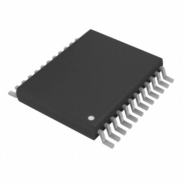
- Package: VSSOP-20
- Essence: This IC is a high-performance, low-voltage CMOS logic gate that provides fast and reliable digital signal processing.
- Packaging/Quantity: Tape and Reel, 2500 units per reel
Specifications
- Supply Voltage Range: 1.65V to 5.5V
- Input Voltage Range: 0V to VCC
- Output Voltage Range: 0V to VCC
- Operating Temperature Range: -40°C to +85°C
- Propagation Delay: 2.8ns (typical)
- Maximum Quiescent Current: 10μA
Detailed Pin Configuration
The SN74LVC821ADGVR has a total of 20 pins arranged as follows:
___________
      |           |
   1  |         20 |  VCC
   2  |         19 |  A1
   3  |         18 |  B1
   4  |         17 |  Y1
   5  |         16 |  GND
   6  |         15 |  A2
   7  |         14 |  B2
   8  |         13 |  Y2
   9  |         12 |  GND
  10  |         11 |  OE#
      |___________|
Functional Features
- Dual 10-bit buffers with 3-state outputs
- Non-inverting outputs
- Output enable control (OE#) for disabling the outputs
- High-speed operation suitable for various digital applications
- Wide operating voltage range allows compatibility with different systems
- Low power consumption for energy-efficient designs
Advantages and Disadvantages
Advantages: - Fast propagation delay ensures quick signal processing - Low-voltage CMOS technology reduces power consumption - Wide operating voltage range provides flexibility in system integration - Small package size saves board space
Disadvantages: - Limited number of input/output pins - Not suitable for high-power applications
Working Principles
The SN74LVC821ADGVR operates based on low-voltage CMOS technology. It consists of two 10-bit buffers with non-inverting outputs. The inputs are buffered to minimize the load on the preceding logic gate, while the outputs can drive standard TTL or CMOS loads.
The output enable control (OE#) pin allows the user to disable the outputs when not needed, reducing power consumption. The IC operates within a wide voltage range, making it compatible with various digital systems.
Detailed Application Field Plans
The SN74LVC821ADGVR is commonly used in the following applications:
- Microcontrollers: Provides level shifting and buffering capabilities between microcontroller pins and other digital components.
- Data Communication Systems: Used for signal conditioning and interfacing in communication protocols such as UART, SPI, and I2C.
- Industrial Automation: Enables reliable digital signal processing in control systems, PLCs, and motor drives.
- Consumer Electronics: Used in audio/video equipment, gaming consoles, and home automation systems for digital signal manipulation.
- Automotive Electronics: Suitable for automotive control units, infotainment systems, and sensor interfaces.
Detailed and Complete Alternative Models
- SN74LVC821APWR: Same functionality and specifications, but available in TSSOP-20 package.
- SN74LVC821ADGV: Same functionality and specifications, but available in SOIC-20 package.
- SN74LVC821ARGYR: Same functionality and specifications, but available in QFN-20 package.
These alternative models provide similar features and can be used as replacements for the SN74LVC821ADGVR based on specific application requirements.
Word count: 529 words
Seznam 10 běžných otázek a odpovědí souvisejících s aplikací SN74LVC821ADGVR v technických řešeních
Sure! Here are 10 common questions and answers related to the application of SN74LVC821ADGVR:
Q: What is SN74LVC821ADGVR? A: SN74LVC821ADGVR is a specific integrated circuit (IC) chip that belongs to the SN74LVC series of logic gates.
Q: What is the function of SN74LVC821ADGVR? A: SN74LVC821ADGVR is an 8-bit D-type flip-flop with 3-state outputs, which means it can store and output digital data.
Q: What voltage levels does SN74LVC821ADGVR support? A: SN74LVC821ADGVR supports voltage levels from 1.65V to 5.5V, making it compatible with a wide range of systems.
Q: How many flip-flops are there in SN74LVC821ADGVR? A: SN74LVC821ADGVR contains 8 individual flip-flops, each capable of storing one bit of data.
Q: Can SN74LVC821ADGVR be used for level shifting? A: Yes, SN74LVC821ADGVR can be used for level shifting as it supports both low-voltage and high-voltage inputs and outputs.
Q: What is the maximum clock frequency supported by SN74LVC821ADGVR? A: SN74LVC821ADGVR can operate at a maximum clock frequency of 100 MHz, allowing for high-speed data processing.
Q: Does SN74LVC821ADGVR have any built-in protection features? A: Yes, SN74LVC821ADGVR has built-in protection against electrostatic discharge (ESD) and excessive power dissipation.
Q: Can SN74LVC821ADGVR be used in battery-powered applications? A: Yes, SN74LVC821ADGVR is suitable for battery-powered applications as it supports low-voltage operation.
Q: What is the typical power consumption of SN74LVC821ADGVR? A: The typical power consumption of SN74LVC821ADGVR is relatively low, making it energy-efficient for various applications.
Q: Are there any application notes or reference designs available for SN74LVC821ADGVR? A: Yes, Texas Instruments provides application notes and reference designs that can help users implement SN74LVC821ADGVR effectively in their technical solutions.
Please note that these answers are general and may vary depending on specific use cases and requirements. It's always recommended to refer to the datasheet and documentation provided by the manufacturer for accurate information.