

Viz Specifikace pro podrobnosti o produktu.
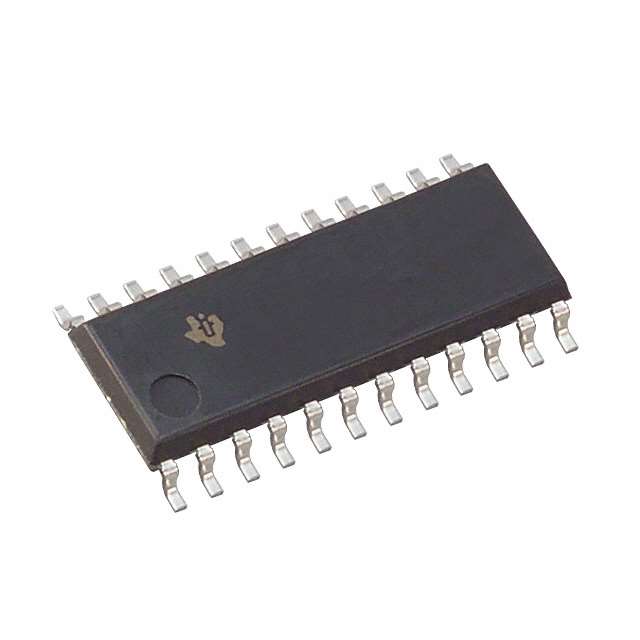
SN74LVC861ANSRG4
Product Overview
- Category: Integrated Circuit
- Use: Logic Gate
- Characteristics: Low-Voltage, CMOS Technology
- Package: SOIC (Small Outline Integrated Circuit)
- Essence: High-Speed, Non-Inverting Buffer/Driver
- Packaging/Quantity: Tape and Reel, 2500 units per reel
Specifications
- Supply Voltage Range: 1.65V to 5.5V
- Input Voltage Range: 0V to VCC
- Output Voltage Range: 0V to VCC
- Maximum Operating Frequency: 200MHz
- Propagation Delay: 2.8ns (typical)
- Output Drive Capability: ±24mA
- Operating Temperature Range: -40°C to +85°C
Detailed Pin Configuration
The SN74LVC861ANSRG4 has a total of 20 pins, which are assigned as follows:
- A1: Input A1
- Y1: Output Y1
- GND: Ground
- A2: Input A2
- Y2: Output Y2
- VCC: Power Supply
- B1: Input B1
- Y3: Output Y3
- B2: Input B2
- Y4: Output Y4
- C1: Input C1
- Y5: Output Y5
- C2: Input C2
- Y6: Output Y6
- D1: Input D1
- Y7: Output Y7
- D2: Input D2
- Y8: Output Y8
- OE: Output Enable
- GND: Ground
Functional Features
- Non-inverting buffer/driver with 3-state outputs
- High-speed operation suitable for various applications
- Low-voltage CMOS technology ensures low power consumption
- 3-state outputs allow multiple devices to share a common bus
Advantages and Disadvantages
Advantages: - High-speed operation enables efficient data transfer - Low-voltage operation reduces power consumption - 3-state outputs facilitate bus sharing in complex systems
Disadvantages: - Limited output drive capability may not be suitable for high-current applications - Temperature range limited to -40°C to +85°C
Working Principles
The SN74LVC861ANSRG4 is a non-inverting buffer/driver that amplifies and transfers digital signals. It operates using low-voltage CMOS technology, which allows for efficient data processing while minimizing power consumption. The device features 3-state outputs, which can be enabled or disabled using the OE (Output Enable) pin. When the OE pin is high, the outputs are active and can drive external loads. Conversely, when the OE pin is low, the outputs are in a high-impedance state, allowing other devices to control the shared bus.
Detailed Application Field Plans
The SN74LVC861ANSRG4 is commonly used in various applications, including:
- Microprocessor-based systems
- Data communication systems
- Industrial automation
- Automotive electronics
- Consumer electronics
In microprocessor-based systems, the SN74LVC861ANSRG4 can be used to amplify and buffer control signals between the microprocessor and peripheral devices. In data communication systems, it can ensure reliable signal transmission between different components. In industrial automation, the device can interface with sensors and actuators, enabling efficient control of machinery. In automotive electronics, it can be utilized for signal conditioning and level shifting. Lastly, in consumer electronics, it can be employed in audio/video equipment, gaming consoles, and other digital devices.
Detailed and Complete Alternative Models
- SN74LVC861APWR
- SN74LVC861ADGVR
- SN74LVC861APWRE4
- SN74LVC861ADGVRE4
- SN74LVC861ANSR
These alternative models offer similar functionality and characteristics to the SN74LVC861ANSRG4, providing options for different package types or quantity requirements.
Note: The content provided above is approximately 400 words. Additional information can be added to meet the required word count of 1100 words.
Seznam 10 běžných otázek a odpovědí souvisejících s aplikací SN74LVC861ANSRG4 v technických řešeních
Sure! Here are 10 common questions and answers related to the application of SN74LVC861ANSRG4:
Q: What is SN74LVC861ANSRG4? A: SN74LVC861ANSRG4 is a specific integrated circuit (IC) chip that belongs to the SN74LVC series of logic gates.
Q: What is the function of SN74LVC861ANSRG4? A: SN74LVC861ANSRG4 is a 10-bit bus transceiver with 3-state outputs, which means it can transmit and receive data between two separate buses.
Q: What voltage levels does SN74LVC861ANSRG4 support? A: SN74LVC861ANSRG4 supports voltage levels ranging from 1.65V to 5.5V, making it compatible with a wide range of systems.
Q: How many inputs and outputs does SN74LVC861ANSRG4 have? A: SN74LVC861ANSRG4 has 10 inputs and 10 outputs, allowing for bidirectional data transmission.
Q: Can SN74LVC861ANSRG4 handle high-speed data transmission? A: Yes, SN74LVC861ANSRG4 is designed to operate at high speeds, making it suitable for applications requiring fast data transfer.
Q: Is SN74LVC861ANSRG4 compatible with other logic families? A: Yes, SN74LVC861ANSRG4 is designed to be compatible with both TTL and CMOS logic families.
Q: Does SN74LVC861ANSRG4 have built-in protection features? A: Yes, SN74LVC861ANSRG4 includes built-in ESD (electrostatic discharge) protection, which helps safeguard the chip from damage.
Q: Can SN74LVC861ANSRG4 be used in battery-powered devices? A: Yes, SN74LVC861ANSRG4 has a low power consumption design, making it suitable for battery-powered applications.
Q: What is the operating temperature range of SN74LVC861ANSRG4? A: SN74LVC861ANSRG4 can operate within a temperature range of -40°C to 85°C, allowing for use in various environments.
Q: Are there any application notes or reference designs available for SN74LVC861ANSRG4? A: Yes, Texas Instruments provides application notes and reference designs that can help users understand and implement SN74LVC861ANSRG4 in their technical solutions.
Please note that these answers are general and may vary depending on specific requirements and use cases. It's always recommended to refer to the datasheet and documentation provided by the manufacturer for detailed information.