

Viz Specifikace pro podrobnosti o produktu.
SN74LVTH125DGVR
Product Overview
- Category: Integrated Circuit (IC)
- Use: Logic Level Translator
- Characteristics: High-speed, low-voltage, and low-power consumption
- Package: VSSOP (Very Small Outline Package)
- Essence: Translates logic levels between different voltage domains
- Packaging/Quantity: Tape and Reel, 2500 units per reel
Specifications
- Supply Voltage Range: 1.65V to 3.6V
- Logic Voltage Levels: 1.8V and 3.3V
- Number of Channels: 4
- Input/Output Type: Tri-State
- Propagation Delay: 2.5ns (typical)
- Operating Temperature Range: -40°C to +85°C
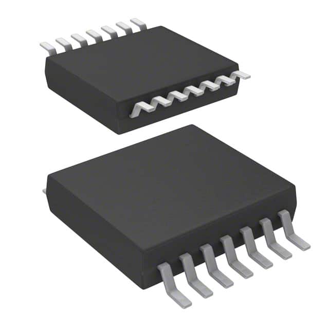
Detailed Pin Configuration
The SN74LVTH125DGVR has a total of 14 pins, which are assigned as follows:
- Pin 1: Output Y1
- Pin 2: Input A1
- Pin 3: Input B1
- Pin 4: GND (Ground)
- Pin 5: Input B2
- Pin 6: Input A2
- Pin 7: Output Y2
- Pin 8: VCC (Supply Voltage)
- Pin 9: Output Y3
- Pin 10: Input A3
- Pin 11: Input B3
- Pin 12: GND (Ground)
- Pin 13: Input B4
- Pin 14: Input A4
Functional Features
- Bidirectional level translation between 1.8V and 3.3V logic signals
- Allows interfacing between devices operating at different voltage levels
- Supports high-speed data transmission
- Tri-state outputs for easy bus sharing
- Low power consumption for energy-efficient applications
Advantages and Disadvantages
Advantages: - Wide supply voltage range allows compatibility with various systems - High-speed operation enables fast data transfer - Tri-state outputs facilitate bus sharing in multi-device systems - Low power consumption extends battery life in portable devices
Disadvantages: - Limited to translating between 1.8V and 3.3V logic levels - Not suitable for applications requiring translation between other voltage domains
Working Principles
The SN74LVTH125DGVR utilizes a combination of MOSFETs and CMOS technology to achieve bidirectional level translation. It employs a voltage divider network to shift the logic levels from one voltage domain to another. The device operates by monitoring the input signal levels and adjusting the output levels accordingly, ensuring proper communication between devices operating at different voltages.
Detailed Application Field Plans
The SN74LVTH125DGVR is commonly used in various applications, including:
- Microcontroller interfacing: Allows communication between microcontrollers operating at different voltage levels.
- Sensor networks: Facilitates data exchange between sensors and control units with varying voltage requirements.
- Industrial automation: Enables integration of different subsystems operating at different voltage domains.
- Battery-powered devices: Provides level translation for efficient power management in portable electronics.
- Communication systems: Supports voltage level conversion in networking equipment and communication protocols.
Detailed and Complete Alternative Models
- SN74LVC1T45DBVR: Single-bit dual-supply voltage level translator with similar characteristics and package.
- SN74AVC4T245PW: Four-bit voltage level translator with tri-state outputs and a wider supply voltage range.
- SN74HCT125N: Quad buffer/line driver with tri-state outputs, suitable for level shifting applications.
These alternative models offer similar functionality and can be considered as substitutes for the SN74LVTH125DGVR based on specific requirements and system constraints.
Word count: 445 words
Seznam 10 běžných otázek a odpovědí souvisejících s aplikací SN74LVTH125DGVR v technických řešeních
Sure! Here are 10 common questions and answers related to the application of SN74LVTH125DGVR:
Question: What is SN74LVTH125DGVR?
- Answer: SN74LVTH125DGVR is a quad bus buffer gate with 3-state outputs, which is commonly used in digital logic circuits.Question: What is the operating voltage range for SN74LVTH125DGVR?
- Answer: The operating voltage range for SN74LVTH125DGVR is typically between 2.7V and 3.6V.Question: What is the maximum output current that SN74LVTH125DGVR can drive?
- Answer: SN74LVTH125DGVR can drive up to 12mA of current per output.Question: Can SN74LVTH125DGVR be used as a level shifter?
- Answer: Yes, SN74LVTH125DGVR can be used as a level shifter to convert signals between different voltage levels.Question: What is the propagation delay of SN74LVTH125DGVR?
- Answer: The propagation delay of SN74LVTH125DGVR is typically around 3.8ns.Question: Can SN74LVTH125DGVR be used in high-speed applications?
- Answer: Yes, SN74LVTH125DGVR is designed for high-speed operation and can be used in applications with fast switching speeds.Question: How many inputs does SN74LVTH125DGVR have?
- Answer: SN74LVTH125DGVR has four independent input channels.Question: Is SN74LVTH125DGVR compatible with other logic families?
- Answer: Yes, SN74LVTH125DGVR is compatible with a wide range of logic families, including TTL, CMOS, and LVTTL.Question: Can SN74LVTH125DGVR be used in bidirectional applications?
- Answer: No, SN74LVTH125DGVR is a unidirectional buffer and cannot be used for bidirectional communication.Question: What is the package type for SN74LVTH125DGVR?
- Answer: SN74LVTH125DGVR is available in a small form factor package called VSSOP-14.
Please note that these answers are general and may vary depending on specific application requirements.