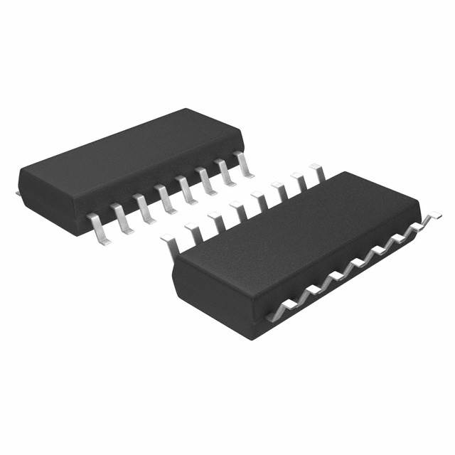
Viz Specifikace pro podrobnosti o produktu.

SN74S139ANSRG4
Product Overview
Category
SN74S139ANSRG4 belongs to the category of integrated circuits (ICs).
Use
This product is commonly used in electronic devices for decoding and demultiplexing applications.
Characteristics
- High-speed operation
- Low power consumption
- Wide operating voltage range
- Compact package size
- RoHS compliant
Package
SN74S139ANSRG4 is available in a small-outline integrated circuit (SOIC) package.
Essence
The essence of SN74S139ANSRG4 lies in its ability to decode and demultiplex input signals, making it an essential component in various electronic systems.
Packaging/Quantity
SN74S139ANSRG4 is typically packaged in reels or tubes, with a quantity of 2500 units per reel/tube.
Specifications
- Supply Voltage: 2V to 6V
- Operating Temperature Range: -40°C to +85°C
- Logic Family: TTL
- Number of Inputs: 2
- Number of Outputs: 4
- Output Type: Active Low
Detailed Pin Configuration
- GND (Ground)
- A0 (Input A0)
- A1 (Input A1)
- Y0 (Output Y0)
- Y1 (Output Y1)
- Y2 (Output Y2)
- Y3 (Output Y3)
- VCC (Supply Voltage)
Functional Features
SN74S139ANSRG4 is designed with the following functional features:
- Decoding: The inputs A0 and A1 are decoded to select one of the four outputs.
- Demultiplexing: The selected output receives the input signal applied to the corresponding input.
Advantages and Disadvantages
Advantages
- High-speed operation allows for efficient signal processing.
- Low power consumption helps in reducing energy usage.
- Wide operating voltage range ensures compatibility with various systems.
- Compact package size enables space-saving designs.
- RoHS compliance promotes environmental sustainability.
Disadvantages
- Limited number of inputs and outputs may restrict its application in complex systems.
- Active low output type may require additional circuitry for certain applications.
Working Principles
SN74S139ANSRG4 operates based on the principles of digital logic. The inputs A0 and A1 are decoded to select one of the four outputs, which then receive the input signal applied to the corresponding input. This decoding and demultiplexing process allows for efficient signal routing and control within electronic systems.
Detailed Application Field Plans
SN74S139ANSRG4 finds applications in various fields, including:
- Communication Systems: Used for signal routing and control in communication devices such as routers and switches.
- Industrial Automation: Enables efficient control and management of signals in industrial automation systems.
- Consumer Electronics: Utilized in devices like televisions and audio systems for signal decoding and distribution.
- Automotive Electronics: Plays a crucial role in automotive systems for signal demultiplexing and control.
Detailed and Complete Alternative Models
Some alternative models that offer similar functionality to SN74S139ANSRG4 include:
- 74HC139N
- CD74HC139E
- MC74HC139AN
- SN74LS139N
These models can be considered as alternatives depending on specific requirements and availability.
Word count: 520 words
Seznam 10 běžných otázek a odpovědí souvisejících s aplikací SN74S139ANSRG4 v technických řešeních
Sure! Here are 10 common questions and answers related to the application of SN74S139ANSRG4 in technical solutions:
Q: What is the SN74S139ANSRG4? A: The SN74S139ANSRG4 is a dual 2-to-4 line decoder/demultiplexer integrated circuit (IC) manufactured by Texas Instruments.
Q: What is the purpose of the SN74S139ANSRG4? A: This IC is used to decode binary information from two input lines into four output lines, making it useful for various digital logic applications.
Q: What is the voltage supply range for the SN74S139ANSRG4? A: The SN74S139ANSRG4 operates with a voltage supply range of 2V to 6V.
Q: How many inputs does the SN74S139ANSRG4 have? A: It has two active-low enable inputs (G1 and G2) and two binary-coded inputs (A and B).
Q: How many outputs does the SN74S139ANSRG4 have? A: It has four outputs (Y0, Y1, Y2, and Y3) that correspond to the decoded binary inputs.
Q: What is the maximum operating frequency of the SN74S139ANSRG4? A: The maximum operating frequency of this IC is typically around 50 MHz.
Q: Can the SN74S139ANSRG4 be cascaded to increase the number of decoded outputs? A: Yes, multiple SN74S139ANSRG4 ICs can be cascaded together to increase the number of decoded outputs.
Q: What is the typical power consumption of the SN74S139ANSRG4? A: The typical power consumption of this IC is relatively low, typically around a few milliwatts.
Q: What are some common applications of the SN74S139ANSRG4? A: This IC is commonly used in address decoding, memory selection, data routing, and other digital logic applications.
Q: Is the SN74S139ANSRG4 available in different package options? A: Yes, it is available in various package options, including SOIC (Small Outline Integrated Circuit) and TSSOP (Thin Shrink Small Outline Package).
Please note that these answers are general and may vary depending on specific datasheet specifications and application requirements.

