

Viz Specifikace pro podrobnosti o produktu.
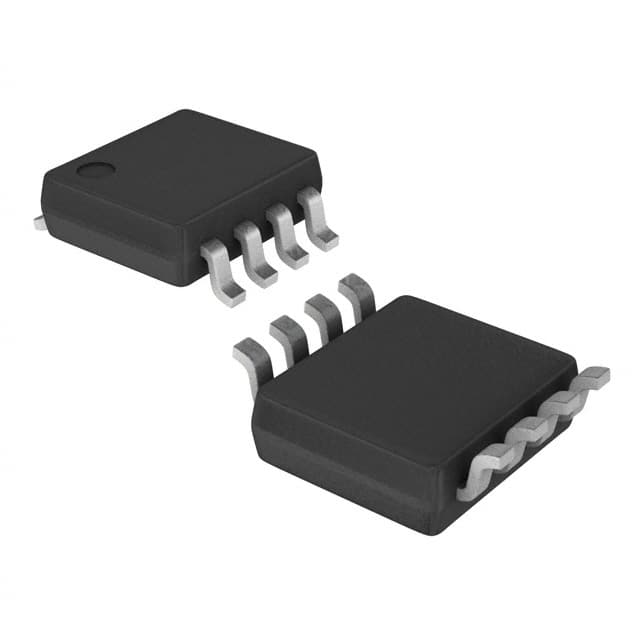
TLV2302IDGK
Product Overview
- Category: Integrated Circuit (IC)
- Use: Operational Amplifier
- Characteristics: Low Voltage, Rail-to-Rail Input/Output, Dual Channel
- Package: MSOP-8
- Essence: TLV2302IDGK is a dual channel operational amplifier designed for low voltage applications with rail-to-rail input and output capabilities.
- Packaging/Quantity: The TLV2302IDGK is available in a MSOP-8 package and is typically sold in reels of 2500 units.
Specifications
- Supply Voltage: 1.8V to 5.5V
- Input Offset Voltage: ±1mV (maximum)
- Gain Bandwidth Product: 1MHz
- Slew Rate: 0.6V/µs
- Input Bias Current: ±1pA (typical)
- Operating Temperature Range: -40°C to +125°C
Pin Configuration
The TLV2302IDGK has a total of 8 pins arranged as follows:
___________
  Vcc | 1       8 | Output A
  In A | 2       7 | In B
  In B | 3       6 | GND
  GND | 4       5 | Output B
       ‾‾‾‾‾‾‾‾‾‾‾
Functional Features
- Low voltage operation allows for compatibility with battery-powered devices.
- Rail-to-rail input/output capability enables the amplifier to handle signals close to the supply rails.
- Dual channel configuration provides flexibility for various applications.
- Low input bias current minimizes the impact on signal integrity.
- Wide operating temperature range allows for use in extreme environments.
Advantages and Disadvantages
Advantages: - Suitable for low voltage applications. - Can handle signals close to the supply rails. - Dual channel configuration provides versatility. - Low input bias current preserves signal integrity. - Wide operating temperature range expands application possibilities.
Disadvantages: - Limited gain bandwidth product compared to some other operational amplifiers. - Slew rate may be slower than desired for certain high-speed applications.
Working Principles
The TLV2302IDGK is based on a differential amplifier architecture. It amplifies the voltage difference between its two input terminals and produces an output voltage proportional to this difference. The rail-to-rail input/output capability ensures that the amplifier can accurately amplify signals that are close to the supply voltage limits.
Detailed Application Field Plans
The TLV2302IDGK is commonly used in various low voltage applications, including but not limited to: - Battery-powered devices - Portable audio equipment - Sensor interfaces - Signal conditioning circuits - Low voltage analog signal processing
Detailed and Complete Alternative Models
Some alternative models that offer similar functionality to the TLV2302IDGK include: - LMV321 - MCP602 - MAX44246 - AD8602 - TS912
These alternatives should be evaluated based on specific requirements and design constraints to determine the most suitable option.
Word count: 311 words
Seznam 10 běžných otázek a odpovědí souvisejících s aplikací TLV2302IDGK v technických řešeních
Sure! Here are 10 common questions and answers related to the application of TLV2302IDGK in technical solutions:
Q: What is TLV2302IDGK? A: TLV2302IDGK is a dual operational amplifier (op-amp) IC that is commonly used in various electronic circuits.
Q: What is the voltage supply range for TLV2302IDGK? A: The voltage supply range for TLV2302IDGK is typically between 2.7V and 5.5V.
Q: What is the maximum output current of TLV2302IDGK? A: TLV2302IDGK has a maximum output current of around 20mA.
Q: Can TLV2302IDGK be used as a comparator? A: Yes, TLV2302IDGK can be used as a comparator, but it is primarily designed as an op-amp.
Q: What is the input offset voltage of TLV2302IDGK? A: The input offset voltage of TLV2302IDGK is typically around 1mV.
Q: Is TLV2302IDGK suitable for low-power applications? A: Yes, TLV2302IDGK is designed for low-power applications and has a low quiescent current consumption.
Q: Can TLV2302IDGK operate in a wide temperature range? A: Yes, TLV2302IDGK is specified to operate in a temperature range of -40°C to +125°C.
Q: What is the typical gain bandwidth product of TLV2302IDGK? A: The typical gain bandwidth product of TLV2302IDGK is around 1MHz.
Q: Can TLV2302IDGK be used in single-supply applications? A: Yes, TLV2302IDGK can be used in single-supply applications as it has rail-to-rail input and output capabilities.
Q: What are some common applications for TLV2302IDGK? A: TLV2302IDGK is commonly used in audio amplifiers, sensor interfaces, signal conditioning circuits, and low-power instrumentation applications.
Please note that the answers provided here are general and may vary depending on specific datasheet specifications and application requirements.