

Viz Specifikace pro podrobnosti o produktu.
TLV5606CDGKR
Product Overview
Category: Integrated Circuit (IC)
Use: TLV5606CDGKR is a digital-to-analog converter (DAC) IC. It converts digital signals into analog voltage outputs.
Characteristics: - High precision and accuracy - Low power consumption - Wide operating temperature range - Fast settling time - Small form factor
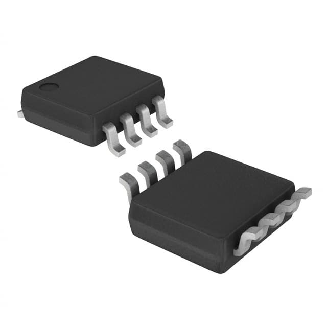
Package: TLV5606CDGKR comes in a small 8-pin VSSOP package, which is suitable for space-constrained applications.
Essence: The TLV5606CDGKR is designed to provide accurate analog voltage outputs based on digital input signals.
Packaging/Quantity: TLV5606CDGKR is typically sold in reels containing 2500 units per reel.
Specifications
- Resolution: 12 bits
- Number of Channels: 1
- Supply Voltage Range: 2.7V to 5.5V
- Output Voltage Range: 0V to Vref
- Operating Temperature Range: -40°C to +125°C
- Digital Interface: Serial Peripheral Interface (SPI)
- Power Consumption: 0.5mW (typical)
Pin Configuration
The TLV5606CDGKR has the following pin configuration:
┌───┐
 VDD │1 8│ VOUT
 SCLK│2 7│ GND
 SDIN│3 6│ LDAC
 CS  │4 5│ REF
   └───┘
- VDD: Supply voltage
- SCLK: Serial clock input
- SDIN: Serial data input
- CS: Chip select input
- REF: Reference voltage input
- LDAC: Load DAC input
- GND: Ground
- VOUT: Analog voltage output
Functional Features
- High-resolution digital-to-analog conversion
- Serial interface for easy integration with microcontrollers and other digital systems
- Internal reference voltage for simplified circuit design
- Load DAC input for simultaneous update of multiple DACs
- Power-down mode for reduced power consumption during idle periods
Advantages and Disadvantages
Advantages: - High precision and accuracy ensure reliable analog outputs - Low power consumption makes it suitable for battery-powered applications - Small form factor allows for space-efficient designs - Wide operating temperature range enables usage in various environments - Fast settling time ensures quick response to digital input changes
Disadvantages: - Limited to a single channel, not suitable for applications requiring multiple independent analog outputs - Requires an external reference voltage source
Working Principles
The TLV5606CDGKR operates by converting digital input signals into corresponding analog voltage outputs. It utilizes a 12-bit resolution to provide precise and accurate analog voltage levels. The digital input signals are received through the serial interface (SCLK and SDIN pins) and converted into analog voltages based on the internal reference voltage (REF pin). The resulting analog voltage is available at the VOUT pin.
Detailed Application Field Plans
The TLV5606CDGKR can be used in various applications, including but not limited to: 1. Audio equipment: Providing analog audio signals for amplifiers, mixers, and audio processing devices. 2. Industrial control systems: Generating analog control signals for motor drives, actuators, and sensors. 3. Test and measurement instruments: Producing precise analog test signals for calibration and testing purposes. 4. Communication systems: Generating analog signals for modulation and demodulation processes. 5. Automotive electronics: Providing analog control signals for automotive systems such as infotainment, climate control, and lighting.
Detailed and Complete Alternative Models
- MCP4921: 12-bit DAC with SPI interface, single channel, similar specifications.
- MAX5216: 16-bit DAC with SPI interface, single channel, higher resolution.
- AD5620: 12-bit DAC with I2C interface, single channel, alternative communication protocol.
These alternative models offer similar functionality to the TLV5606CDGKR and can be considered based on specific application requirements.
Word count: 529 words
Seznam 10 běžných otázek a odpovědí souvisejících s aplikací TLV5606CDGKR v technických řešeních
Sure! Here are 10 common questions and answers related to the application of TLV5606CDGKR:
Q: What is TLV5606CDGKR? A: TLV5606CDGKR is a 12-bit digital-to-analog converter (DAC) with a voltage reference and serial interface, commonly used in technical solutions.
Q: What is the operating voltage range of TLV5606CDGKR? A: The operating voltage range of TLV5606CDGKR is typically between 2.7V and 5.5V.
Q: What is the resolution of TLV5606CDGKR? A: TLV5606CDGKR has a resolution of 12 bits, which means it can provide 4096 different output voltage levels.
Q: What is the maximum output current of TLV5606CDGKR? A: The maximum output current of TLV5606CDGKR is typically around 2 mA.
Q: Does TLV5606CDGKR have an internal voltage reference? A: Yes, TLV5606CDGKR has an internal voltage reference of 2.5V, which can be used as a reference for the DAC output voltage.
Q: Can TLV5606CDGKR operate in both single-ended and differential modes? A: Yes, TLV5606CDGKR can operate in both single-ended and differential modes, depending on the application requirements.
Q: What is the serial interface used by TLV5606CDGKR? A: TLV5606CDGKR uses a standard SPI (Serial Peripheral Interface) for communication with microcontrollers or other devices.
Q: Is TLV5606CDGKR suitable for low-power applications? A: Yes, TLV5606CDGKR is designed for low-power operation and has a power-down mode to minimize power consumption when not in use.
Q: Can TLV5606CDGKR be used in industrial applications? A: Yes, TLV5606CDGKR is suitable for industrial applications due to its wide operating voltage range and robust design.
Q: Are there any evaluation boards or development kits available for TLV5606CDGKR? A: Yes, Texas Instruments provides evaluation boards and development kits for TLV5606CDGKR, which can help with prototyping and testing in various applications.
Please note that the answers provided here are general and may vary depending on specific datasheet specifications and application requirements.