

Viz Specifikace pro podrobnosti o produktu.
TLV5606IDGKRG4
Product Overview
- Category: Integrated Circuit (IC)
- Use: Digital-to-Analog Converter (DAC)
- Characteristics: High-resolution, low-power consumption
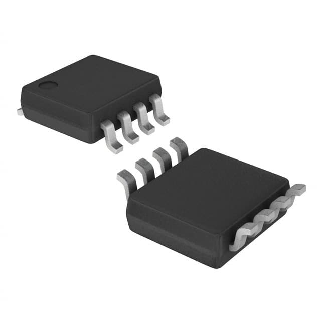
- Package: VSSOP-8
- Essence: Converts digital signals into analog voltage or current
- Packaging/Quantity: Tape and Reel, 2500 units per reel
Specifications
- Resolution: 16-bit
- Number of Channels: 1
- Supply Voltage Range: 2.7V to 5.5V
- Operating Temperature Range: -40°C to +125°C
- Output Type: Voltage or Current
- Output Range: 0V to Vref or 4mA to 20mA
- Interface: Serial Peripheral Interface (SPI)
Pin Configuration
The TLV5606IDGKRG4 has the following pin configuration:
┌───┬───┐
   │ 1 │ 8 │
   │   │   │
   │   │   │
   │   │   │
   │   │   │
   │   │   │
   │   │   │
   │ 4 │ 5 │
   └───┴───┘
Pin Description: 1. VDD: Power supply voltage input 2. GND: Ground reference 3. DIN: Serial data input 4. CS: Chip select input 5. SCLK: Serial clock input 6. REF: Reference voltage input 7. AGND: Analog ground reference 8. OUT: Analog output
Functional Features
- High-resolution DAC with 16-bit resolution
- Low power consumption for energy-efficient applications
- Wide supply voltage range allows flexibility in system design
- Serial interface enables easy integration with microcontrollers and other digital devices
- Output can be configured as voltage or current, providing versatility in application
Advantages and Disadvantages
Advantages: - High resolution allows for precise analog signal generation - Low power consumption extends battery life in portable devices - Flexible supply voltage range accommodates various power sources - Serial interface simplifies communication with digital systems
Disadvantages: - Limited to a single channel output - Requires external reference voltage for accurate conversion
Working Principles
The TLV5606IDGKRG4 is a digital-to-analog converter (DAC) that converts digital signals into analog voltage or current. It utilizes a 16-bit resolution to provide high precision in the conversion process. The input digital data is received through the serial peripheral interface (SPI), and the DAC generates the corresponding analog output based on the received data. The output can be configured as either a voltage or a current, depending on the application requirements. The TLV5606IDGKRG4 operates within a wide supply voltage range and consumes low power, making it suitable for a variety of applications.
Detailed Application Field Plans
The TLV5606IDGKRG4 finds applications in various fields, including:
- Audio Equipment: Used in audio amplifiers and mixers to convert digital audio signals into analog signals for playback.
- Industrial Automation: Integrated into control systems to generate analog control signals for motor speed control, valve positioning, and other industrial processes.
- Test and Measurement Instruments: Employed in oscilloscopes, function generators, and data acquisition systems to produce accurate analog waveforms for testing and analysis.
- Communication Systems: Utilized in wireless transceivers and base stations to generate analog signals for modulation and demodulation processes.
- Automotive Electronics: Incorporated into automotive infotainment systems, climate control units, and engine management systems for analog signal generation.
Detailed and Complete Alternative Models
- DAC8562: 16-bit DAC with dual channels and SPI interface.
- MCP4922: 12-bit DAC with dual channels and SPI interface.
- MAX5216: 16-bit DAC with single channel and I2C interface.
- AD5662: 16-bit DAC with single channel and SPI interface.
- LTC2630: 12-bit DAC with single channel and I2C interface.
These alternative models offer similar functionality to the TLV5606IDGKRG4 and can be considered based on specific application requirements.
Word count: 550 words
Seznam 10 běžných otázek a odpovědí souvisejících s aplikací TLV5606IDGKRG4 v technických řešeních
Sure! Here are 10 common questions and answers related to the application of TLV5606IDGKRG4:
Q: What is TLV5606IDGKRG4? A: TLV5606IDGKRG4 is a 12-bit digital-to-analog converter (DAC) that converts digital data into analog voltage signals.
Q: What is the operating voltage range of TLV5606IDGKRG4? A: The operating voltage range of TLV5606IDGKRG4 is typically between 2.7V and 5.5V.
Q: What is the maximum output voltage range of TLV5606IDGKRG4? A: The maximum output voltage range of TLV5606IDGKRG4 is typically between 0V and Vref, where Vref is the reference voltage.
Q: Can TLV5606IDGKRG4 be used in both single-ended and differential configurations? A: Yes, TLV5606IDGKRG4 can be used in both single-ended and differential configurations, depending on the application requirements.
Q: What is the resolution of TLV5606IDGKRG4? A: TLV5606IDGKRG4 has a resolution of 12 bits, which means it can represent 2^12 (4096) different voltage levels.
Q: Does TLV5606IDGKRG4 have an internal voltage reference? A: No, TLV5606IDGKRG4 does not have an internal voltage reference. An external reference voltage must be provided.
Q: What is the typical settling time of TLV5606IDGKRG4? A: The typical settling time of TLV5606IDGKRG4 is around 10µs, which refers to the time it takes for the output voltage to stabilize after a change in the digital input.
Q: Can TLV5606IDGKRG4 be used in industrial applications? A: Yes, TLV5606IDGKRG4 is suitable for industrial applications as it can operate over a wide temperature range and has good noise performance.
Q: What is the power supply current requirement of TLV5606IDGKRG4? A: The power supply current requirement of TLV5606IDGKRG4 depends on the operating conditions but typically ranges from 0.5mA to 2.5mA.
Q: Is TLV5606IDGKRG4 available in a surface-mount package? A: Yes, TLV5606IDGKRG4 is available in a surface-mount package with the DGK (VSSOP-8) package type.
Please note that the answers provided here are general and may vary depending on specific datasheet specifications and application requirements.