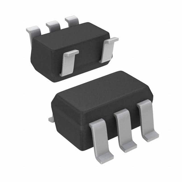
Viz Specifikace pro podrobnosti o produktu.

TPS61041DBVR
Product Overview
Category
The TPS61041DBVR belongs to the category of integrated circuits (ICs) and specifically falls under the voltage regulators - switching regulators classification.
Use
This product is primarily used for boosting or stepping up voltage levels in various electronic applications. It is commonly employed in portable devices, such as smartphones, tablets, and digital cameras, where efficient power management is crucial.
Characteristics
- High efficiency: The TPS61041DBVR offers excellent power conversion efficiency, minimizing energy loss during voltage conversion.
- Wide input voltage range: It can operate with input voltages ranging from 1.8V to 6V, providing flexibility in different power supply scenarios.
- Adjustable output voltage: The device allows users to set the desired output voltage level within a specific range, catering to diverse application requirements.
- Low quiescent current: The TPS61041DBVR features low standby current consumption, contributing to extended battery life in portable devices.
- Thermal shutdown protection: It incorporates a thermal shutdown mechanism that safeguards the IC from overheating, ensuring reliable operation.
Package and Quantity
The TPS61041DBVR is available in a small SOT-23-5 package, which is compact and suitable for space-constrained designs. It is typically sold in reels containing 3000 units per reel.
Specifications
- Input Voltage Range: 1.8V to 6V
- Output Voltage Range: Adjustable from 2.5V to 5.5V
- Maximum Output Current: 100mA
- Switching Frequency: 1.2MHz
- Operating Temperature Range: -40°C to 85°C
- Quiescent Current: 30µA (typical)
Pin Configuration
The TPS61041DBVR has five pins arranged as follows:
```
| | --| VIN GND |-- Pin 1: VIN (Input Voltage) --| EN SW |-- Pin 2: EN (Enable) --| FB NC |-- Pin 3: FB (Feedback) --| PGND SW |-- Pin 4: PGND (Power Ground) --| VOUT SW |-- Pin 5: VOUT (Output Voltage) |___________| ```
Functional Features
- Enable (EN) Pin: This pin controls the device's operation. When a logic high signal is applied, the TPS61041DBVR is enabled and starts boosting the input voltage. Conversely, a logic low signal disables the device, reducing power consumption.
- Feedback (FB) Pin: The FB pin is used to set the desired output voltage level. By connecting external resistors or a voltage divider network, users can adjust the output voltage within the specified range.
- Power Ground (PGND): This pin serves as the ground reference for the internal power stage of the IC.
- Input Voltage (VIN): The VIN pin receives the input voltage that needs to be boosted.
- Output Voltage (VOUT): The VOUT pin provides the boosted output voltage.
Advantages and Disadvantages
Advantages
- High efficiency leads to reduced power loss during voltage conversion.
- Wide input voltage range allows compatibility with various power sources.
- Adjustable output voltage caters to different application requirements.
- Low quiescent current extends battery life in portable devices.
- Thermal shutdown protection ensures reliable operation.
Disadvantages
- Limited maximum output current may not be suitable for high-power applications.
- SOT-23-5 package may pose challenges in heat dissipation for certain designs.
Working Principles
The TPS61041DBVR operates as a boost converter, utilizing a switching regulator topology. When enabled, it converts the input voltage to a higher output voltage level by controlling the switching of an internal power transistor. This switching action, coupled with an inductor and capacitor, efficiently steps up the voltage while minimizing energy loss.
Detailed Application Field Plans
The TPS61041DBVR finds applications in various portable electronic devices, including but not limited to: - Smartphones - Tablets - Digital cameras - Portable media players - Wearable devices
Detailed and Complete Alternative Models
- TPS61042DBVR: Similar to TPS61041DBVR, but with a higher maximum output current of 200mA.
- TPS61043DBVR: Offers adjustable output voltage range from 1.8V to 6V, suitable for wider application scenarios.
- TPS61044DBVR: Provides higher efficiency and lower quiescent current compared to TPS61041DBVR.
These alternative models offer similar functionality with slight variations in specifications, catering to different design requirements.
Word count: 570 words
Seznam 10 běžných otázek a odpovědí souvisejících s aplikací TPS61041DBVR v technických řešeních
Sure! Here are 10 common questions and answers related to the application of TPS61041DBVR in technical solutions:
Q: What is TPS61041DBVR? A: TPS61041DBVR is a boost converter integrated circuit (IC) designed for applications requiring a regulated output voltage higher than the input voltage.
Q: What is the input voltage range of TPS61041DBVR? A: The input voltage range of TPS61041DBVR is typically between 0.9V and 6V.
Q: What is the output voltage range of TPS61041DBVR? A: The output voltage range of TPS61041DBVR can be adjusted from 1.8V to 5.5V.
Q: What is the maximum output current of TPS61041DBVR? A: The maximum output current of TPS61041DBVR is typically 100mA.
Q: Can TPS61041DBVR operate with a single lithium-ion battery as the input source? A: Yes, TPS61041DBVR can efficiently boost the voltage from a single lithium-ion battery to power various applications.
Q: Does TPS61041DBVR have built-in protection features? A: Yes, TPS61041DBVR includes over-temperature protection, over-current protection, and under-voltage lockout to ensure safe operation.
Q: Can TPS61041DBVR be used in portable devices such as smartphones or tablets? A: Yes, TPS61041DBVR is suitable for powering portable devices that require a higher voltage than the battery's output.
Q: Is TPS61041DBVR easy to use in a circuit design? A: Yes, TPS61041DBVR is a simple and straightforward IC to implement in circuit designs due to its minimal external component requirements.
Q: Can TPS61041DBVR operate at high efficiency? A: Yes, TPS61041DBVR has a high efficiency of up to 90%, making it suitable for battery-powered applications that require power conservation.
Q: Are there any application notes or reference designs available for TPS61041DBVR? A: Yes, Texas Instruments provides application notes and reference designs that can help users understand and implement TPS61041DBVR effectively in their technical solutions.
Please note that the answers provided here are general and may vary depending on specific design considerations and requirements. It is always recommended to refer to the datasheet and relevant documentation for accurate information.

