

Viz Specifikace pro podrobnosti o produktu.
XC6118C39DGR-G
Product Overview
Category
XC6118C39DGR-G belongs to the category of voltage regulators.
Use
It is commonly used in electronic circuits to regulate and stabilize voltage levels.
Characteristics
- Voltage regulation
- Stabilization of voltage levels
- Compact size
- Low power consumption
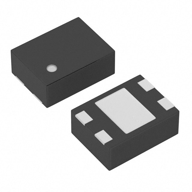
Package
XC6118C39DGR-G comes in a small surface-mount package.
Essence
The essence of XC6118C39DGR-G lies in its ability to provide stable voltage output for various electronic devices.
Packaging/Quantity
XC6118C39DGR-G is typically packaged in reels or tubes, with a quantity of 3000 units per reel/tube.
Specifications
- Input Voltage Range: 2.5V - 6.0V
- Output Voltage: 3.9V
- Output Current: 150mA
- Dropout Voltage: 200mV (typical)
- Quiescent Current: 30μA (typical)
- Operating Temperature Range: -40°C to +85°C
Detailed Pin Configuration
XC6118C39DGR-G has the following pin configuration:
- VIN (Input Voltage)
- GND (Ground)
- VOUT (Output Voltage)
Functional Features
- Voltage Regulation: XC6118C39DGR-G ensures a stable output voltage regardless of input voltage fluctuations.
- Overcurrent Protection: It incorporates overcurrent protection to safeguard connected devices.
- Low Power Consumption: The regulator operates with low quiescent current, minimizing power consumption.
Advantages and Disadvantages
Advantages
- Compact size allows for easy integration into space-constrained designs.
- Wide input voltage range provides flexibility in various applications.
- Low dropout voltage minimizes power dissipation.
- Overcurrent protection ensures the safety of connected devices.
Disadvantages
- Limited output current may not be suitable for high-power applications.
- Operating temperature range may restrict usage in extreme environments.
Working Principles
XC6118C39DGR-G utilizes a feedback mechanism to maintain a constant output voltage. It compares the output voltage with a reference voltage and adjusts the internal circuitry accordingly to regulate the output voltage within the specified range.
Detailed Application Field Plans
XC6118C39DGR-G finds applications in various electronic devices, including but not limited to: - Mobile phones - Portable audio players - Digital cameras - Wearable devices - IoT devices
Detailed and Complete Alternative Models
Some alternative models that can be considered as alternatives to XC6118C39DGR-G are: - LM317T - LT1084CP-5 - LM7805 - AMS1117-3.3
These models offer similar voltage regulation capabilities and can be used as substitutes depending on specific requirements.
Word count: 320 words
Seznam 10 běžných otázek a odpovědí souvisejících s aplikací XC6118C39DGR-G v technických řešeních
Sure! Here are 10 common questions and answers related to the application of XC6118C39DGR-G in technical solutions:
Q: What is XC6118C39DGR-G? A: XC6118C39DGR-G is a voltage detector IC (integrated circuit) that monitors the power supply voltage and provides a reset signal when the voltage drops below a certain threshold.
Q: What is the operating voltage range of XC6118C39DGR-G? A: The operating voltage range of XC6118C39DGR-G is typically between 0.9V and 6.0V.
Q: How does XC6118C39DGR-G help in technical solutions? A: XC6118C39DGR-G helps in technical solutions by providing a reliable reset signal to microcontrollers, microprocessors, or other digital circuits when the power supply voltage falls below a specified level, ensuring proper system initialization.
Q: What is the typical reset voltage threshold of XC6118C39DGR-G? A: The typical reset voltage threshold of XC6118C39DGR-G is 3.9V.
Q: Can XC6118C39DGR-G be used in battery-powered applications? A: Yes, XC6118C39DGR-G can be used in battery-powered applications as it has a low quiescent current consumption of typically 1.0µA, making it suitable for power-sensitive designs.
Q: Does XC6118C39DGR-G have any built-in delay time for the reset signal? A: Yes, XC6118C39DGR-G has a built-in delay time of typically 200ms to ensure stable power supply before releasing the reset signal.
Q: Can XC6118C39DGR-G be used in automotive applications? A: Yes, XC6118C39DGR-G is suitable for automotive applications as it meets the AEC-Q100 Grade 2 qualification standards.
Q: What is the package type of XC6118C39DGR-G? A: XC6118C39DGR-G is available in a small SOT-25 package, which is compact and easy to integrate into various designs.
Q: Is XC6118C39DGR-G compatible with both CMOS and TTL logic levels? A: Yes, XC6118C39DGR-G is compatible with both CMOS and TTL logic levels, making it versatile for different digital circuit applications.
Q: Are there any additional features or protections provided by XC6118C39DGR-G? A: Yes, XC6118C39DGR-G includes features like hysteresis, short-circuit protection, and reverse current protection, enhancing its reliability and robustness in various technical solutions.
Please note that the answers provided here are general and may vary depending on the specific datasheet and application requirements.